A method and device for preparing a p-type doped amorphous silicon thin film
A technology of amorphous silicon thin film and preparation device, which is applied in the direction of final product manufacturing, sustainable manufacturing/processing, ion implantation and plating, etc., can solve the problem of low doping efficiency of P-type amorphous silicon thin film and low doping efficiency thin film defects And other issues
- Summary
- Abstract
- Description
- Claims
- Application Information
AI Technical Summary
Problems solved by technology
Method used
Image


Examples
Embodiment 1
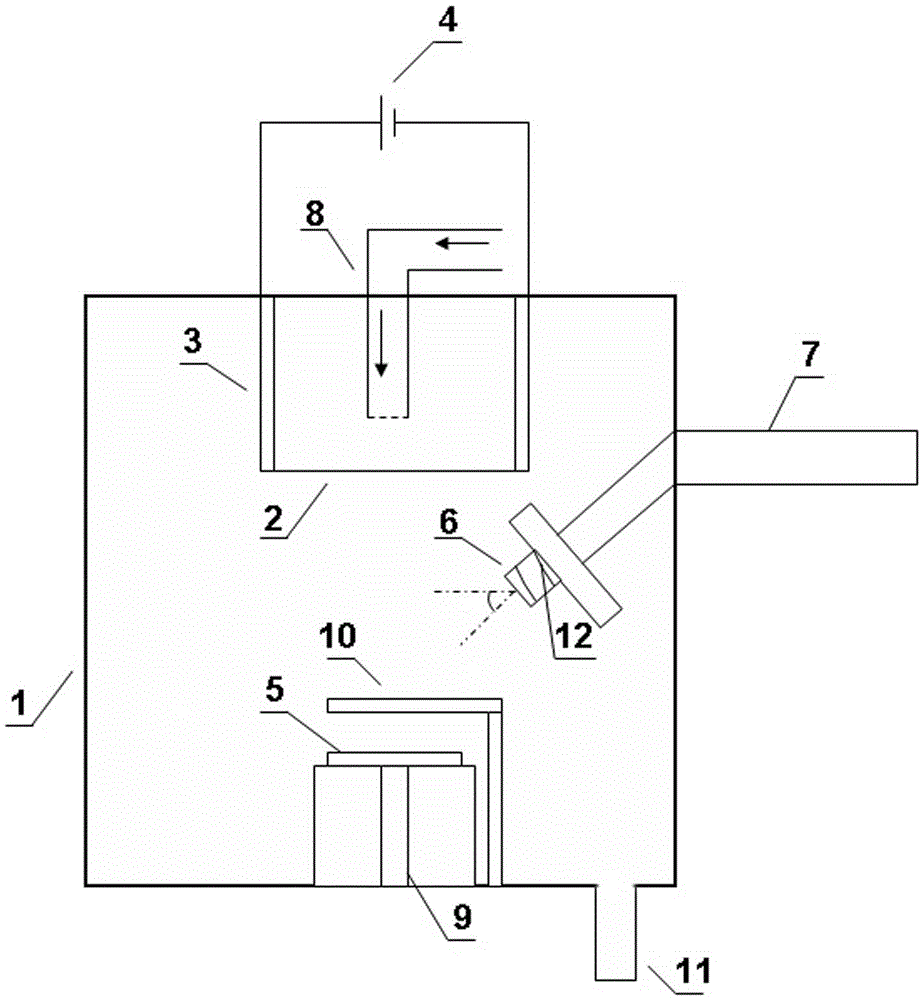
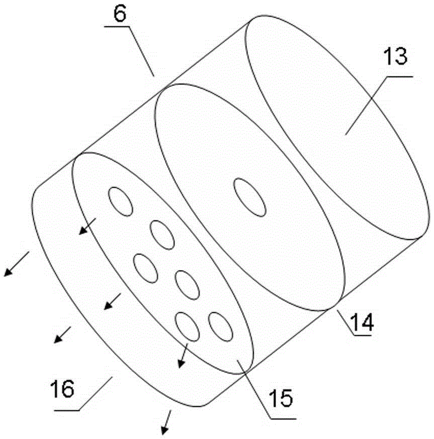
[0015] (1) adopt figure 1 In the shown device, the distance between the tantalum wire 2 and the substrate plate 5 is 10 cm, the angle between the surface normal of the ceramic crucible 6 and the plane of the substrate plate 5 is 80° C., and the aluminum source used in the thermal reaction evaporator 7 is 99.9999% aluminum purity;
[0016] (2) Put the AZO conductive glass on the substrate plate 5 in the vacuum chamber 1, and use the vacuum pump 11 to evacuate the vacuum chamber so that the vacuum degree of the vacuum chamber is 1×10 -4 Pa, and the temperature of the substrate plate 5 is controlled to be 200° C. by the substrate heater 9;
[0017] (3) Feed the mixed reaction gas hydrogen and silane into the vacuum chamber at the same time, the flow ratio of hydrogen and silane is 1:1, apply voltage to the tantalum wire 2 to heat, so that the temperature of the tantalum wire 2 reaches 1750°C, and the flow rate of the gas is controlled Make the pressure of the reaction gas in th...
Embodiment 2
[0022] (1) adopt figure 1 In the shown device, the distance between the tantalum wire 2 and the substrate plate 5 is 12 cm, the angle between the surface normal of the ceramic crucible 6 and the substrate plate plane is 75° C., and the purity of the aluminum source used in the thermal reaction evaporator 7 is 99.9999% Aluminum;
[0023] (2) Put the AZO conductive glass on the substrate plate 5 of the vacuum chamber 1, and use the vacuum pump 11 to evacuate the vacuum chamber so that the vacuum degree of the vacuum chamber is 1×10 -4 Pa, and the temperature of the substrate plate 5 is controlled to be 200° C. by the substrate heater 9;
[0024] (3) Feed the mixed reaction gas hydrogen and silane into the vacuum chamber at the same time, the flow ratio of hydrogen and silane is 1.2:1, apply voltage to the tantalum wire 2 to heat, so that the temperature of the tantalum wire 2 reaches 1700 ° C, through the flow control of the gas Make the pressure of the reaction gas in the vac...
Embodiment 3
[0029] (1) adopt figure 1 In the shown device, the distance between the tantalum wire 2 and the substrate plate 5 is 15 cm, the angle between the surface normal of the ceramic crucible 6 and the substrate plate plane is 85° C., and the purity of the aluminum source used in the thermal reaction evaporator 7 is 99.9999% Aluminum;
[0030] (2) Put the AZO conductive glass on the substrate plate 5 in the vacuum chamber 1, and use the vacuum pump 11 to evacuate the vacuum chamber so that the vacuum degree of the vacuum chamber is 1×10 -4 Pa, and the temperature of the substrate plate 5 is controlled to be 200° C. by the substrate heater 9;
[0031] (3) Feed the mixed reaction gas hydrogen and silane into the vacuum chamber at the same time, the flow ratio of hydrogen and silane is 1.5:1, apply voltage to the tantalum wire 2 to heat, so that the temperature of the tantalum wire 2 reaches 1750°C, and the flow rate of the gas is controlled Make the pressure of the reaction gas in the ...
PUM
| Property | Measurement | Unit |
|---|---|---|
| diameter | aaaaa | aaaaa |
| thickness | aaaaa | aaaaa |
Abstract
Description
Claims
Application Information
 - R&D
- Intellectual Property
- Life Sciences
- Materials
- Tech Scout
- Unparalleled Data Quality
- Higher Quality Content
- 60% Fewer Hallucinations
Browse by: Latest US Patents, China's latest patents, Technical Efficacy Thesaurus, Application Domain, Technology Topic, Popular Technical Reports.
© 2025 PatSnap. All rights reserved.Legal|Privacy policy|Modern Slavery Act Transparency Statement|Sitemap|About US| Contact US: help@patsnap.com