A metal dielectric layer and its manufacturing method and a circuit board

A technology for dielectric layers and circuit boards, applied to circuits, printed circuit components, electrical components, etc., can solve problems such as interface cracks and aluminum wires falling off

Active Publication Date: 2015-08-19
FOUNDER MICROELECTRONICS INT
View PDF7 Cites 0 Cited by
  • Summary
  • Abstract
  • Description
  • Claims
  • Application Information

AI Technical Summary

Problems solved by technology

[0009] The present application provides a metal dielectric layer located on a pad of a circuit board, a manufacturing method thereof, and a circuit board, which are used to solve problems in the metal dielectric layer caused by stress generated during the wire pressing process in the prior art. The interface between the spin-on-glass layer and the dielectric layer is broken, and the technical problem of aluminum wire falling off

Method used


Image

  • A metal dielectric layer and its manufacturing method and a circuit board
  • A metal dielectric layer and its manufacturing method and a circuit board
  • A metal dielectric layer and its manufacturing method and a circuit board

Examples


Embodiment Construction

[0043] In order to enable those skilled in the technical field to which the application belongs to understand the application more clearly, the technical solutions of the application will be described in detail below through specific embodiments in conjunction with the accompanying drawings.

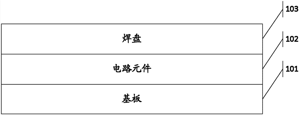
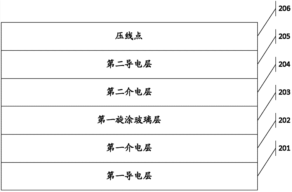
[0044] Please refer to figure 1 , figure 2 , Embodiment 1 of the present application provides a circuit board, such as figure 1 As shown, the circuit board specifically includes the following structure:

[0045] Substrate 101;

[0046] At least one pad 103, through which at least one circuit element 102 is connected to other circuits; the pad 103 includes:

[0047] The first conductive layer 201 and the second conductive layer 205;

[0048] In a specific implementation process, the two conductive layers can be made of metal or other conductive materials, and the material is not limited to metal. In addition, the conductive layer can be two layers, or multiple layers.

[0049] The ...


PUM


Abstract

The invention discloses a metal dielectric layer, a manufacturing method thereof and a circuit board. The circuit board structurally comprises a substrate, at least one bonding pad and at least one circuit component. The circuit component is connected with other circuits through the bonding pad. The bonding pad comprises a first conducting layer, a second conducting layer, wire pressing points and the metal dielectric layer. The wire pressing points are arranged on the upper surface of the second conducting layer. The metal dielectric layer is located between the first conducting layer and the second conducting layer. The metal dielectric layer comprises a first dielectric layer, a first spin-coating glass layer and a second dielectric layer. The first dielectric layer is arranged on the upper surface of the first conducting layer. The first spin-coating glass layer is arranged on the upper surface of the first dielectric layer. The first spin-coating glass layer is the spin-coating glass layer containing arsenic. The second dielectric layer is located on the upper surface of the first spin-coating glass layer.

Description

technical field [0001] The present application relates to the technical field of semiconductors, in particular to a metal dielectric layer, a manufacturing method thereof, and a circuit board. Background technique [0002] With the rapid development of semiconductor technology, especially with the development of integrated circuits, the requirements for integrated circuits are becoming increasingly sophisticated and complex. In order to reduce costs, the current common integrated circuit packaging method is COB (chip on board: chip on board packaging), which is to adhere the bare chip to the interconnection substrate with conductive or non-conductive adhesive, and then perform wire bonding to realize its electrical connection. connect. In the COB packaging process, the key technology lies in wire bonding (Wire Bonding). Wire bonding refers to the use of aluminum wire bonding machines to connect the chip (LED die or IC chip) to the corresponding PCB board (printed circuit bo...

Claims


Application Information

Patent Timeline
Patent Type & Authority Patents(China)
IPC IPC(8): H01L23/498H05K1/11H01L21/60
CPCH01L2924/0002
Inventor 陈建国李天贺贺冠中
Owner FOUNDER MICROELECTRONICS INT
Why Eureka
Try Eureka