Linear stabilizer with low pressure difference
A low dropout linear, voltage regulator technology, applied in instruments, regulating electrical variables, control/regulating systems, etc., can solve the problem of increasing circuit-level design scale, increasing circuit complexity and cost, increasing static power consumption and circuit low frequency Noise and other problems, to achieve the effect of saving layout area, improving overshoot and undershoot, and low overall power consumption
- Summary
- Abstract
- Description
- Claims
- Application Information
AI Technical Summary
Problems solved by technology
Method used
Image
Examples
Embodiment 1
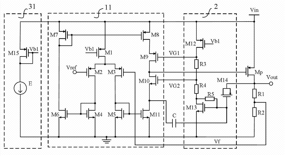
[0030] Such as image 3 As shown, a low-dropout linear regulator includes: a bias voltage generation circuit 31, an error amplifier 11, an output transistor Mp, a compensation capacitor C and a fast response circuit 2; the output transistor Mp is a PMOS transistor, and its source is connected to the input Voltage Vin; where:
[0031] The bias voltage generation circuit 31 is used to provide the bias voltage Vb1 to the error amplifier 11 and the fast response circuit 2; in this embodiment, the bias voltage generation circuit 31 is composed of a PMOS transistor M15 and a current source E; wherein, the PMOS transistor M15 The source is connected to the input voltage Vin, the gate and drain of the PMOS transistor M15 are connected to one end of the current source E to generate a bias voltage Vb1, and the other end of the current source E is grounded.
[0032] The fast response circuit 2 is used to sense the load transient step by collecting the output voltage Vout of the output t...
Embodiment 2
[0040] Such as Figure 4 As shown, a low-dropout linear regulator includes: a bias voltage generating circuit 32, an error amplifier 12, an output transistor Mp, a compensation capacitor C and a fast response circuit 2; the output transistor Mp is a PMOS transistor, and its source is connected to the input Voltage Vin; where:
[0041] The bias voltage generating circuit 32 is used to provide bias voltages Vb1 and Vb2 to the fast response circuit 2 and the error amplifier 12 respectively; in this embodiment, the bias voltage generating circuit 32 is composed of a PMOS transistor M15, an NMOS transistor M16 and a current source E ; wherein, the source of the PMOS transistor M15 is connected to the input voltage Vin, the gate and drain of the PMOS transistor M15 are connected to one end of the current source E to generate a bias voltage Vb1, and the other end of the current source E is connected to the drain of the NMOS transistor M16 It is connected to the gate and generates a ...
PUM
 Abstract
Description
Claims
Application Information
 - R&D
- Intellectual Property
- Life Sciences
- Materials
- Tech Scout
- Unparalleled Data Quality
- Higher Quality Content
- 60% Fewer Hallucinations
Browse by: Latest US Patents, China's latest patents, Technical Efficacy Thesaurus, Application Domain, Technology Topic, Popular Technical Reports.
© 2025 PatSnap. All rights reserved.Legal|Privacy policy|Modern Slavery Act Transparency Statement|Sitemap|About US| Contact US: help@patsnap.com


