Image display device and image display method
An image display device, image display panel technology, applied in image communication, static indicators, cathode ray tube indicators, etc., can solve the problem of less charging time, increased module power consumption, gate drive, and data line drive frequency Changes increase and other issues, to achieve the effect of reducing power consumption, reducing frequency changes, and ensuring charging time
- Summary
- Abstract
- Description
- Claims
- Application Information
AI Technical Summary
Problems solved by technology
Method used
Image
Examples
Embodiment 1
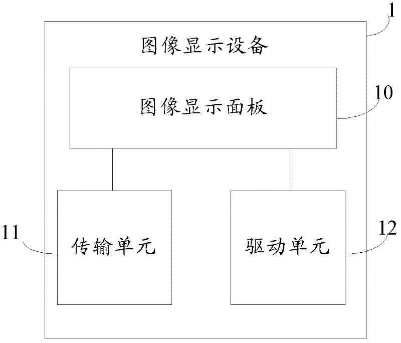
[0030] An image display device 1 provided by an embodiment of the present invention, such as figure 1 shown, including:
[0031] The image display panel 10 is used for displaying 2D images or 3D images by a plurality of combined pixels.
[0032] Each combined pixel in the image display panel 10 includes a first row of sub-pixels, and a second row of sub-pixels located below the first row of sub-pixels and forming a combined sub-pixel together with the first row of sub-pixels, and for each row of combined For a pixel, the first gate wiring is connected to the first row of sub-pixels, and the second gate wiring is connected to the second row of sub-pixels.
[0033] It should be noted that a plurality of combined pixels form the image display panel 10 according to m rows and n columns, and each row of sub-pixels includes the first row of sub-pixels and the second row of sub-pixels. In this implementation, the transmission unit is used to transmit 2D display data and 3D display d...
Embodiment 2
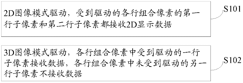
[0055] The image display method provided by the embodiment of the present invention is used to drive an image display device. The display device includes m columns and n rows of combined sub-pixels, each combined pixel includes a first row of sub-pixels, and sub-pixels located in the first row Below, and together with the first row of sub-pixels, the second row of sub-pixels that constitute the combined sub-pixels, and for each row of combined pixels, the first gate wiring is connected to the first row of sub-pixels, and the second gate wiring is connected to the second row of sub-pixels pixels, such as figure 2 shown, including the following steps:
[0056] It is worth pointing out that there is no sequence relationship between the following steps S101 and S102, and they can be performed simultaneously or successively. Wherein, if it is necessary to switch from the 2D image mode to the 3D image mode, it can be performed in the order of S101 and S102.
[0057] It should be n...
PUM
 Abstract
Description
Claims
Application Information
 - R&D
- Intellectual Property
- Life Sciences
- Materials
- Tech Scout
- Unparalleled Data Quality
- Higher Quality Content
- 60% Fewer Hallucinations
Browse by: Latest US Patents, China's latest patents, Technical Efficacy Thesaurus, Application Domain, Technology Topic, Popular Technical Reports.
© 2025 PatSnap. All rights reserved.Legal|Privacy policy|Modern Slavery Act Transparency Statement|Sitemap|About US| Contact US: help@patsnap.com


