Methods for manufacturing dielectric layer and organic electroluminescent device
A manufacturing method and dielectric layer technology, applied in the fields of electric solid-state devices, semiconductor/solid-state device manufacturing, electrical components, etc., can solve problems such as loss and inability to excite surface plasma waves
- Summary
- Abstract
- Description
- Claims
- Application Information
AI Technical Summary
Problems solved by technology
Method used
Image

Examples
Embodiment Construction
[0040] In order to make the above objects, features and advantages of the present invention more comprehensible, specific implementations of the present invention will be described in detail below in conjunction with the accompanying drawings.
[0041] In the following description, a lot of specific details are set forth in order to fully understand the present invention, but the present invention can also be implemented in other ways different from those described here, and those skilled in the art can do it without departing from the meaning of the present invention. By analogy, the present invention is therefore not limited to the specific examples disclosed below.
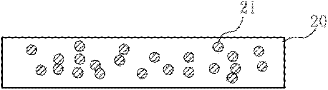
[0042] See figure 1 , figure 1 It is a schematic structural view of the dielectric layer of the organic electroluminescent device of the present invention, and the dielectric layer includes: a dielectric layer body 20 and metal nanostructure particles 21 inside the dielectric layer body 20 .
[0043] The diel...
PUM
 Abstract
Description
Claims
Application Information
 - R&D
- Intellectual Property
- Life Sciences
- Materials
- Tech Scout
- Unparalleled Data Quality
- Higher Quality Content
- 60% Fewer Hallucinations
Browse by: Latest US Patents, China's latest patents, Technical Efficacy Thesaurus, Application Domain, Technology Topic, Popular Technical Reports.
© 2025 PatSnap. All rights reserved.Legal|Privacy policy|Modern Slavery Act Transparency Statement|Sitemap|About US| Contact US: help@patsnap.com