Printable semiconductor structures and related methods of making and assembling
A semiconductor and overall technology, applied in semiconductor/solid-state device manufacturing, semiconductor devices, transistors, etc., can solve problems such as destruction, cracking, and damage
- Summary
- Abstract
- Description
- Claims
- Application Information
AI Technical Summary
Problems solved by technology
Method used
Image

Examples
Embodiment 1
[0107] Example 1 Aligned GaAs line arrays for flexible transistors, diodes and circuits printed on plastic substrates
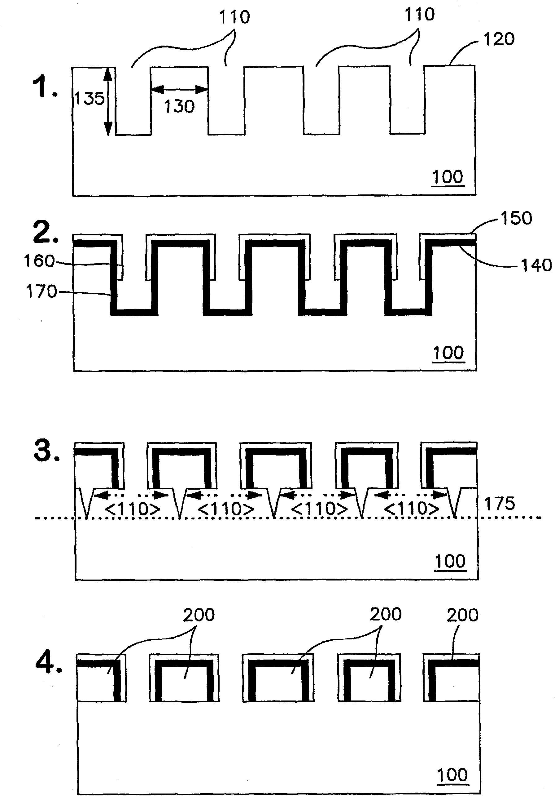
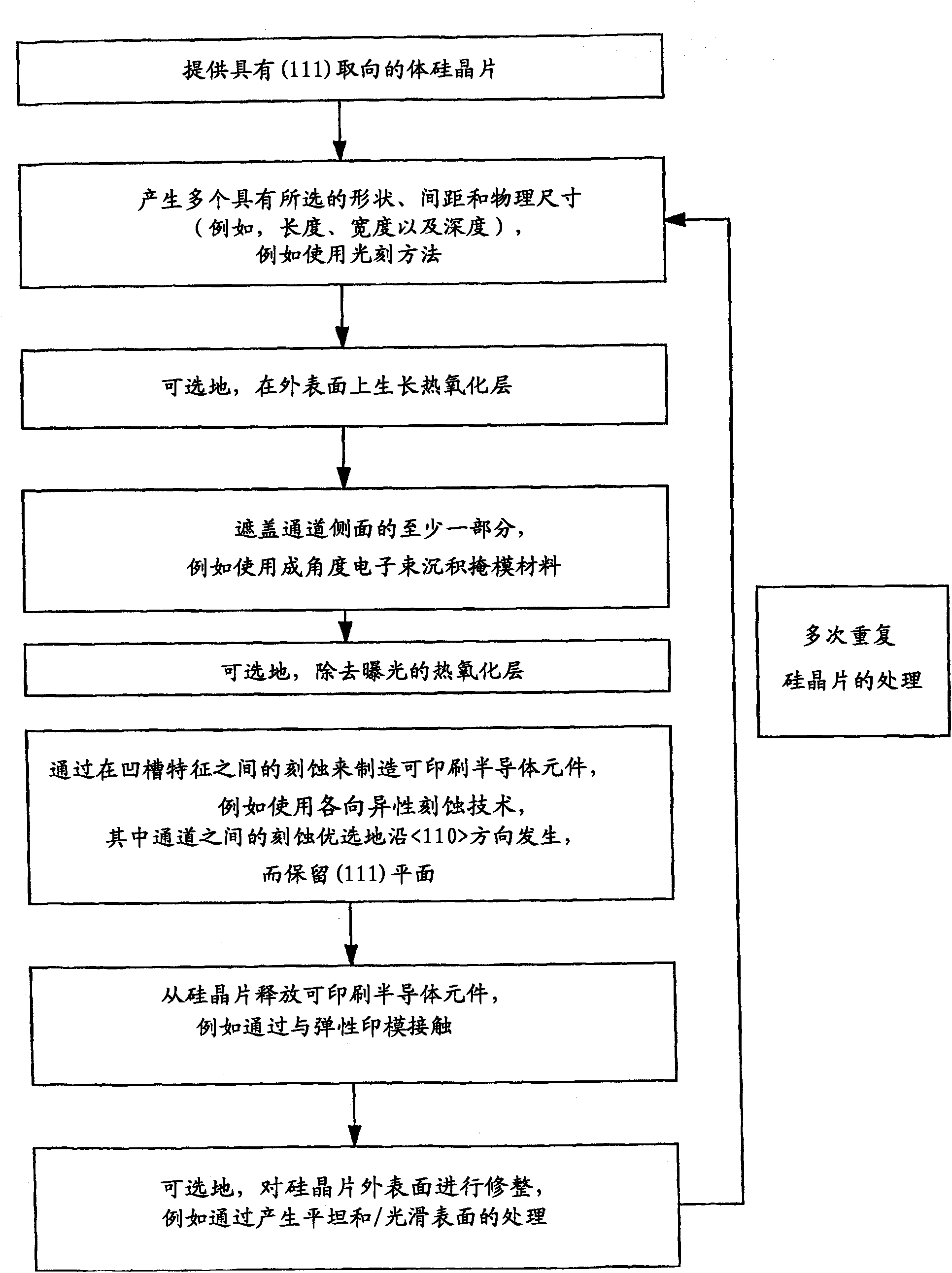
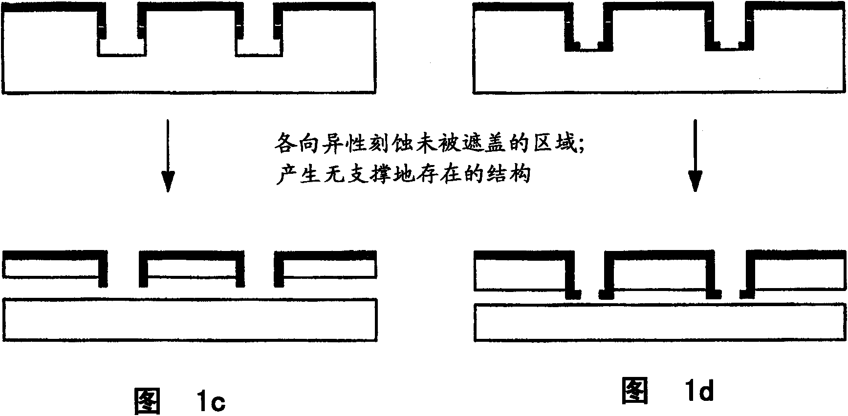
[0108] GaAs line-aligned arrays with integrated ohmic contacts produced from high-quality single-crystal wafers using photolithography and anisotropic chemical etching provide a promising transistor for use on flexible plastic substrates, Materials for Schottky diodes, logic gates, and even more complex circuits. These devices exhibit excellent electrical and mechanical properties, both of which are important for the emerging field of low-cost, large-area flexible electronics, often called macroelectronics.
[0109] Micro- and nano-scale wires, ribbons, platelets, etc. of single-crystalline inorganic semiconductors are attractive for functional devices (e.g., optical devices, optoelectronic devices, electronic devices, sensor devices, etc.) that can be used in many applications. The building block of force. For example, Si nanowires synthesized by a "bottom...
Embodiment 2
[0121] Example 2: Gigahertz operation of a mechanically flexible transistor on a flexible plastic substrate
[0122] The combined use of GaAs wires with ohmic contacts formed from bulk wafers, soft lithographic transfer printing techniques, and optimized device designs enables the formation of mechanically flexible transistors on low-cost plastic substrates with individual device speeds in the gigahertz range and with High mechanical bendability. The methods disclosed herein include materials that are fabricated with limited lithographic image forming resolution and registration in a simple layout. This example describes the electrical and mechanical properties of high performance transistors. These results are of great importance in certain applications including, but not limited to, high-speed communications and computing, and emerging types of large-area electronic systems ("macroelectronic devices").
[0123] Large-area flexible electronic systems (ie, macroelectronic de...
Embodiment 3
[0145] In summary, the results of this example show that surface stresses (up to 0.71% in tension and compression) induced by bending do not significantly degrade the performance of MESFETs fabricated by the modified process. More importantly, releasing the sample in the bent state restored the device performance to its original state. These observations indicate that GaAs wire-based MESFETs on PU / PET substrates have mechanical properties that meet the requirements for many envisioned macroelectronic device applications. In addition, these types of TFTs exhibit high speeds approaching those suitable for RF communications equipment and other applications requiring mechanical flexibility, lightweight construction, and compatibility with large-area, printing-like processing. speed. GaAs has some of the same disadvantages as Si used in conventional integrated circuits (i.e. high wafer cost) for devices using thin, bendable wires or ribbons of suitable density and large area circu...
PUM
 Abstract
Description
Claims
Application Information
 - R&D Engineer
- R&D Manager
- IP Professional
- Industry Leading Data Capabilities
- Powerful AI technology
- Patent DNA Extraction
Browse by: Latest US Patents, China's latest patents, Technical Efficacy Thesaurus, Application Domain, Technology Topic.
© 2024 PatSnap. All rights reserved.Legal|Privacy policy|Modern Slavery Act Transparency Statement|Sitemap