Display repairing method and display structure after being repaired
A display and post-repair technology, which can be used in instruments, nonlinear optics, optics, etc., and can solve problems such as unsatisfactory effects and ink falling off
- Summary
- Abstract
- Description
- Claims
- Application Information
AI Technical Summary
Problems solved by technology
Method used
Image
Examples
Embodiment Construction
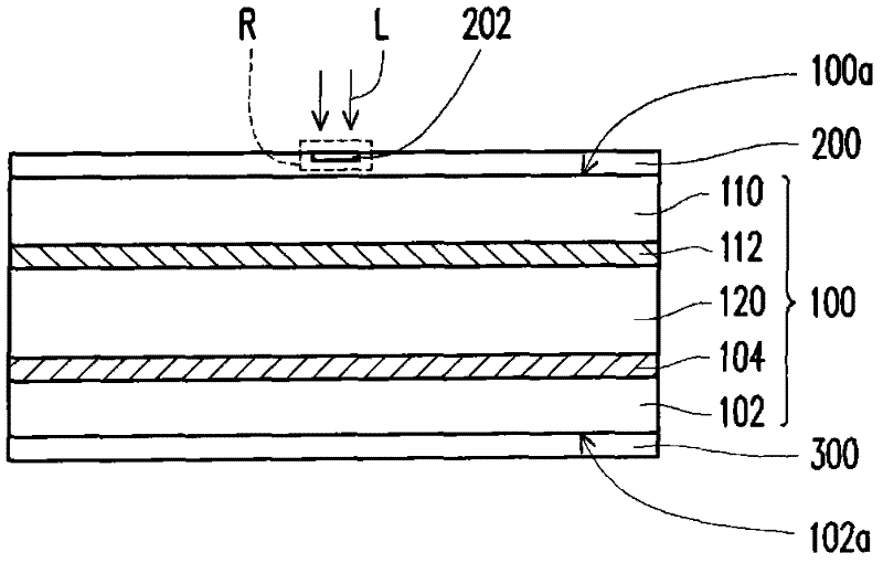
[0015] figure 1 It is a schematic cross-sectional view of a display repair method according to an embodiment of the present invention. Please refer to figure 1 , the repairing method of this embodiment first provides a display, and the display includes a display panel 100 and at least one optical film 200 , 300 .
[0016] The display panel 100 includes a first substrate 102 , a pixel array layer 104 , a second substrate 110 , an electrode layer / color filter layer 112 and a display medium 120 .
[0017] The first substrate 102 and the second substrate 110 are arranged opposite to each other, and the materials of the first substrate 102 and the second substrate 110 can be glass, quartz, organic polymer, or opaque / reflective materials (for example: conductive materials, metal, silicon wafer, ceramics, or other applicable materials), or other applicable materials.
[0018] The pixel array layer 104 is disposed on the first substrate 102 . The pixel array layer 104 includes a p...
PUM
| Property | Measurement | Unit |
|---|---|---|
| wavelength | aaaaa | aaaaa |
| thickness | aaaaa | aaaaa |
| size | aaaaa | aaaaa |
Abstract
Description
Claims
Application Information
 - Generate Ideas
- Intellectual Property
- Life Sciences
- Materials
- Tech Scout
- Unparalleled Data Quality
- Higher Quality Content
- 60% Fewer Hallucinations
Browse by: Latest US Patents, China's latest patents, Technical Efficacy Thesaurus, Application Domain, Technology Topic, Popular Technical Reports.
© 2025 PatSnap. All rights reserved.Legal|Privacy policy|Modern Slavery Act Transparency Statement|Sitemap|About US| Contact US: help@patsnap.com


