
Control method for extension slice equability for 6 inch As back lining MOS part

A technology of MOS devices and control methods, which is applied in semiconductor/solid-state device manufacturing, electrical components, circuits, etc., can solve problems such as unsatisfactory self-doping, unsatisfactory edge uniformity, and unfavorable mass production, etc. time, reduce process time, and reduce production cost

Active Publication Date: 2009-07-01
HEBEI POSHING ELECTRONICS TECH
View PDF2 Cites 1 Cited by
  • Summary
  • Abstract
  • Description
  • Claims
  • Application Information

AI Technical Summary

Problems solved by technology

The time of this method of gas removal is the method that has been used all the time. The time of gas removal is the same for two times. This not only wastes a lot of time, but also the control of self-doping is not very ideal, which is extremely unfavorable for mass production.
6-inch self-doping is more serious than 4-inch, and the control of edge uniformity is far from ideal

Method used

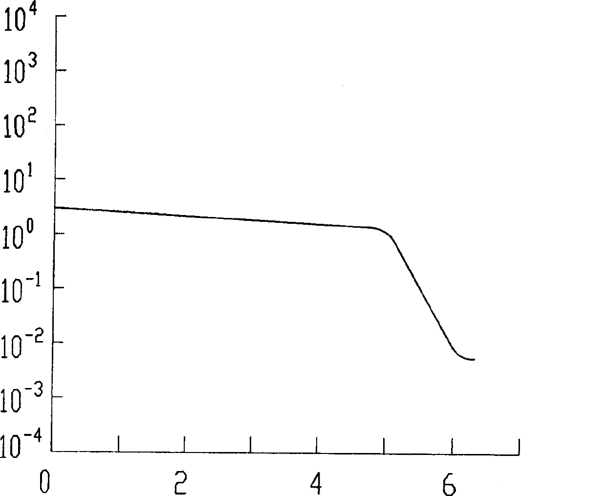
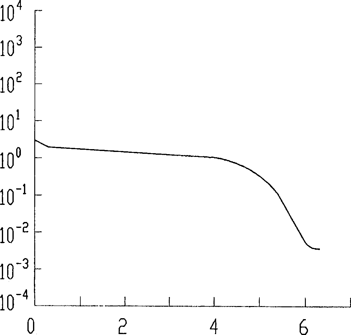

Image

  • Control method for extension slice equability for 6 inch As back lining MOS part
  • Control method for extension slice equability for 6 inch As back lining MOS part

Examples


Embodiment 1

[0037] 1. Substrate requirements: the following table.

[0038]

Parameter

Unit (unit)

Specification

value

(standard value) Dopant Arsenic / arsenic Resistivity (resistivity) CM 0.002-0.004 RRGMAX

(resistivity radial gradient position)

25.0 Orientation Degree (degree) 1-1-1 Off Orientation

(Deviation of crystal orientation) Degree (degree)

4.0°±0.5°

Thickness and thickness

tolerance

(thickness and tolerance)

Microns (microns)

6260±20.0

Diameter and diametrical

tolerance

(diameter and tolerance)

mm (mm)

150.0±0.20

Backside (back) A 5000±500

[0039] 2. Extension parameters

[0040] The resistivity of the epitaxial layer is 24±8%Ω·cm, and the thickness of the epitaxial layer is 50±5%μm.

[0041] 3. The epitaxial equipment used

[0042] The PE2061 epitaxial furnace of Italy LPE Company is adopted, and each furnace can hold 14 p...

Embodiment 2

[0051] The difference between this embodiment and the embodiment is that: the first time in the process 4.2 with large flow H 2 The flushing time is 30 minutes; the second time in 4.5 with large flow of H 2 Rinse and catch air for 5 minutes.

Embodiment 3

[0053] The difference between this embodiment and the embodiment is that: the first time in the process 4.2 with large flow H 2 The flushing time is 25 minutes; the second time in 4.5 with large flow of H 2 Rinse and catch the air, the time is 7 minutes.


PUM


Abstract

The invention discloses a method for controlling the uniformity of a 6-inch As backsealing substrate MOS device epitaxial wafer. This method uses the process steps of HCL in-situ polishing—the first high-flow H2 degassing—cooling—growth intrinsic layer—the second high-flow H2 degassing—the process method of growing an epitaxial layer with remaining thickness. The time for the first high-flow H2 gas flushing is 25-30 minutes, and the second high-flow H2 gas flushing time is 5-10 minutes. After many tests, it is found that the present invention is the best gas-catch time, which can effectively control self-doping and improve the edge uniformity of the resistivity of the epitaxial sheet. Both the flatness of the extended resistance and the steepness of the transition region of the epitaxial wafer obtained by the method of the present invention are more ideal than those of the epitaxial wafer obtained by the traditional method.

Description

technical field [0001] The invention relates to a production method of MOS device epitaxial wafers, in particular to a method for controlling the uniformity of MOS device epitaxial wafers with a 6-inch As backsealing substrate. Background technique [0002] Silicon epitaxial wafer is the main material for making semiconductor discrete devices, because it can not only ensure the high breakdown voltage of PN junction, but also reduce the forward voltage drop of the device. At the same time, silicon epitaxial wafer is the main material of bipolar integrated circuit (IC). Manufacturing process, it can not only make IC devices on the lightly doped epitaxial layer with heavily doped buried layer, but also form a grown PN junction, which solves the isolation problem of IC. Making CMOS circuits with silicon epitaxial wafers can suppress latch-up (Latchup) effect and resist soft errors generated by alpha particles, so silicon epitaxial wafers are increasingly used in CMOS devices. I...

Claims


Application Information

Patent Timeline
Patent Type & Authority Patents(China)
IPC IPC(8): H01L21/02H01L21/20
Inventor 薛宏伟
Owner HEBEI POSHING ELECTRONICS TECH
Learn More