Power converter
a technology of power converters and cooling fins, applied in power conversion systems, instruments, ac network circuit arrangements, etc., can solve the problems of too high cooling capability of cooling fins, and achieve the effect of equalizing the loss occurring in semiconductor devices
- Summary
- Abstract
- Description
- Claims
- Application Information
AI Technical Summary
Benefits of technology
Problems solved by technology
Method used
Image
Examples
first embodiment
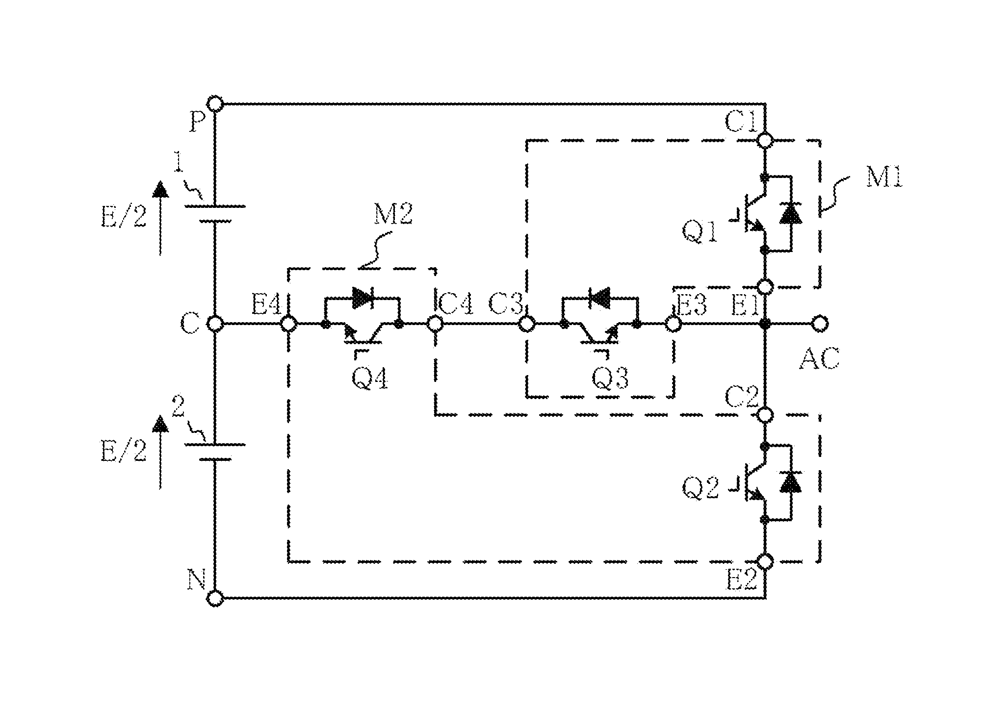
[0032]FIG. 1 is a diagram for illustrating the power converter according to the invention.
[0033]In FIG. 1, the semiconductor device M1 has four terminals, terminals C1, E1, C3, and E3, for connecting to an external circuit. The terminal C1 is connected to the collector terminal of the semiconductor switching element Q1, while the terminal E1 is connected to the emitter terminal. Also, the terminal C3 is connected to the collector terminal of the semiconductor switching element Q3, while the terminal E3 is connected to the emitter terminal. Then, the collector terminal and the emitter terminal of the semiconductor switching element Q1 and the collector terminal and the emitter terminal of the semiconductor switching element Q3 are each isolated.
[0034]Meanwhile, the semiconductor device M2 has four terminals, terminals C2, E2, C4, and E4, for connecting to an external circuit. The terminal C2 is connected to the collector terminal of the semiconductor switching element Q2, while the t...
second embodiment
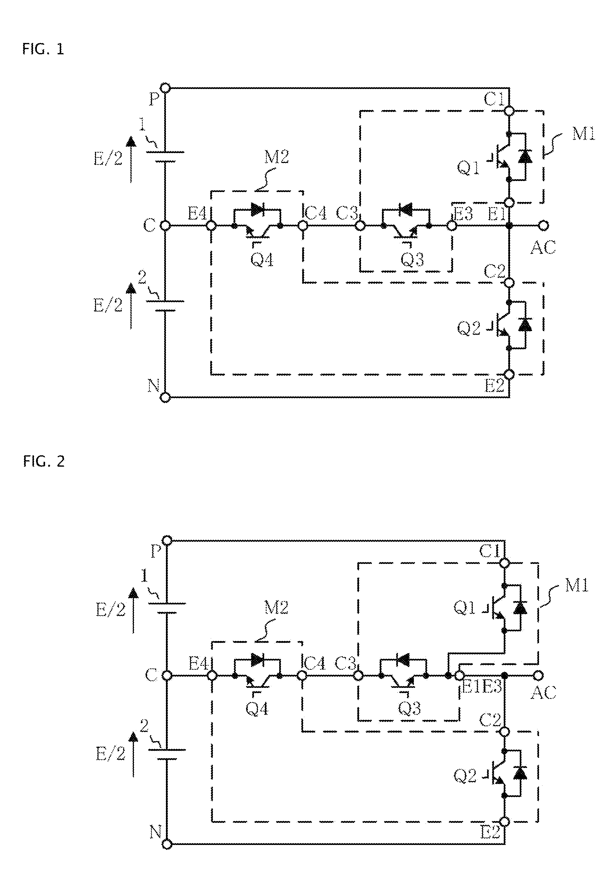
[0038]FIG. 2 is a diagram for illustrating the power converter according to the invention.
[0039]In FIG. 2, the semiconductor device M1 has three terminals, terminals C1, E1E3, and C3, for connecting to an external circuit. The terminal C1 is connected to the collector terminal of the semiconductor switching element Q1, while the terminal C3 is connected to the collector terminal of the semiconductor switching element Q3. Then, the emitter terminal of the semiconductor switching element Q1 and the emitter terminal of the semiconductor switching element Q3 are connected inside the semiconductor device M1. This connection point is connected to the terminal E1E3 for connection to an external circuit.
[0040]Meanwhile, the semiconductor device M2, in the same way as the semiconductor device M2 of FIG. 1, has four terminals, and the configuration thereof is also the same.
[0041]Next, the first series circuit is a circuit wherein the semiconductor switching element Q1 of the semiconductor dev...
third embodiment
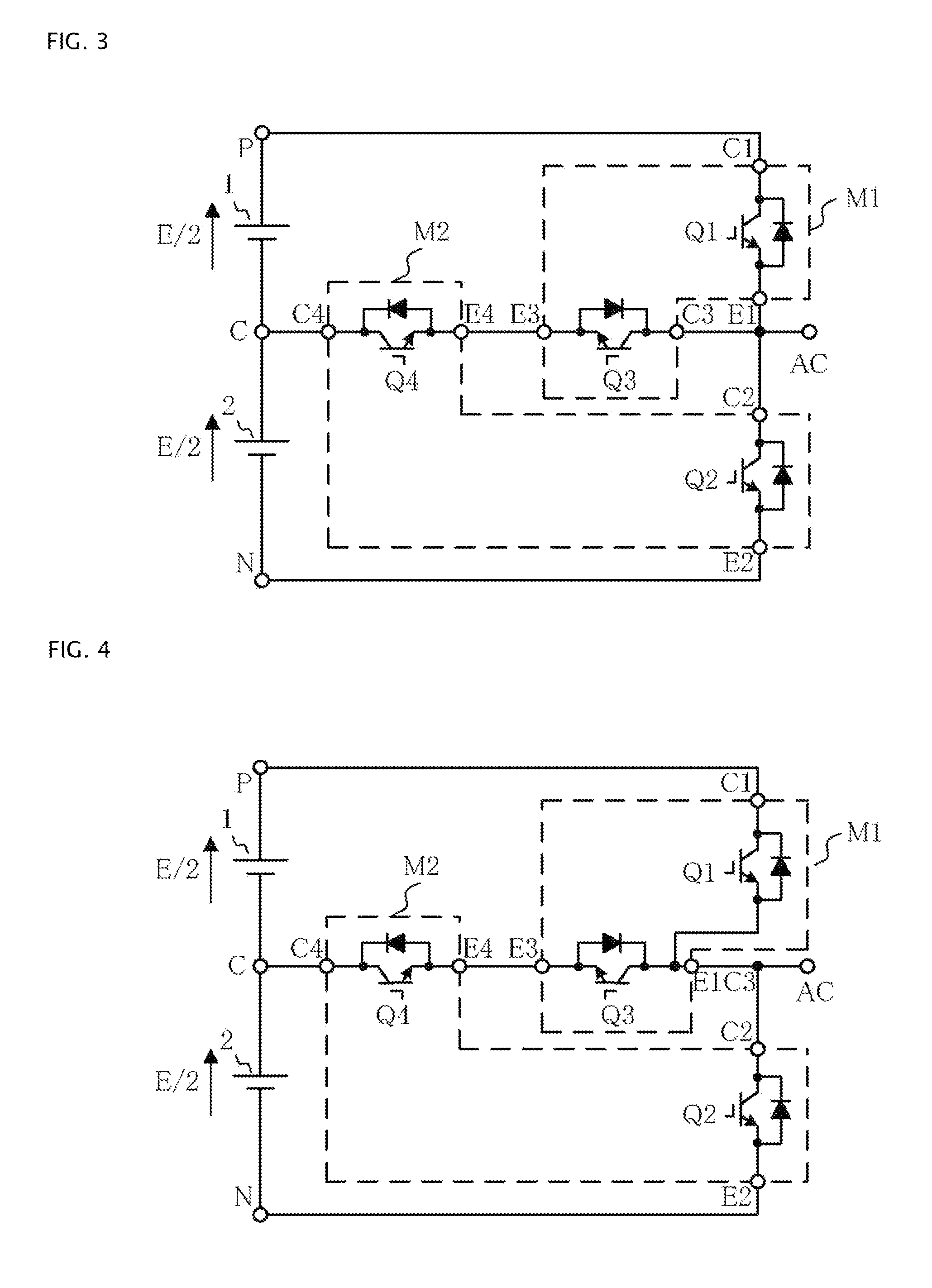
[0044]FIG. 3 is a diagram for illustrating the power converter according to the invention.
[0045]In FIG. 3, each of the semiconductor devices M1 and M2, in the same way as the semiconductor devices M1 and M2 shown in FIG. 1, has four terminals, and the configuration thereof is also the same.
[0046]Also, the first series circuit is also the same as the first series circuit shown in FIG. 1.
[0047]The second series circuit is a circuit wherein the semiconductor switching element Q3 of the semiconductor device M1 and the semiconductor switching element Q4 of the semiconductor device M2 are connected in anti-series. In order to configure the second series circuit, the terminal E3 of the semiconductor device M1 and the terminal E4 of the semiconductor device M2 are connected. By so doing, the semiconductor switching element Q3 and the semiconductor switching element Q4 are connected in anti-series. Also, the terminal C3 of the semiconductor device M1 is connected to the connection point of t...
PUM
 Abstract
Description
Claims
Application Information
 - R&D
- Intellectual Property
- Life Sciences
- Materials
- Tech Scout
- Unparalleled Data Quality
- Higher Quality Content
- 60% Fewer Hallucinations
Browse by: Latest US Patents, China's latest patents, Technical Efficacy Thesaurus, Application Domain, Technology Topic, Popular Technical Reports.
© 2025 PatSnap. All rights reserved.Legal|Privacy policy|Modern Slavery Act Transparency Statement|Sitemap|About US| Contact US: help@patsnap.com


