
Protective self-aligned buffer layers for damascene interconnects

a buffer layer and self-aligning technology, applied in the direction of chemical vapor deposition coating, semiconductor/solid-state device details, coatings, etc., can solve the problems of metal electromigration drop, improve adhesion, improve the effect of damascene interconnects

Active Publication Date: 2013-04-30
NOVELLUS SYSTEMS
View PDF63 Cites 9 Cited by
  • Summary
  • Abstract
  • Description
  • Claims
  • Application Information

AI Technical Summary

Benefits of technology

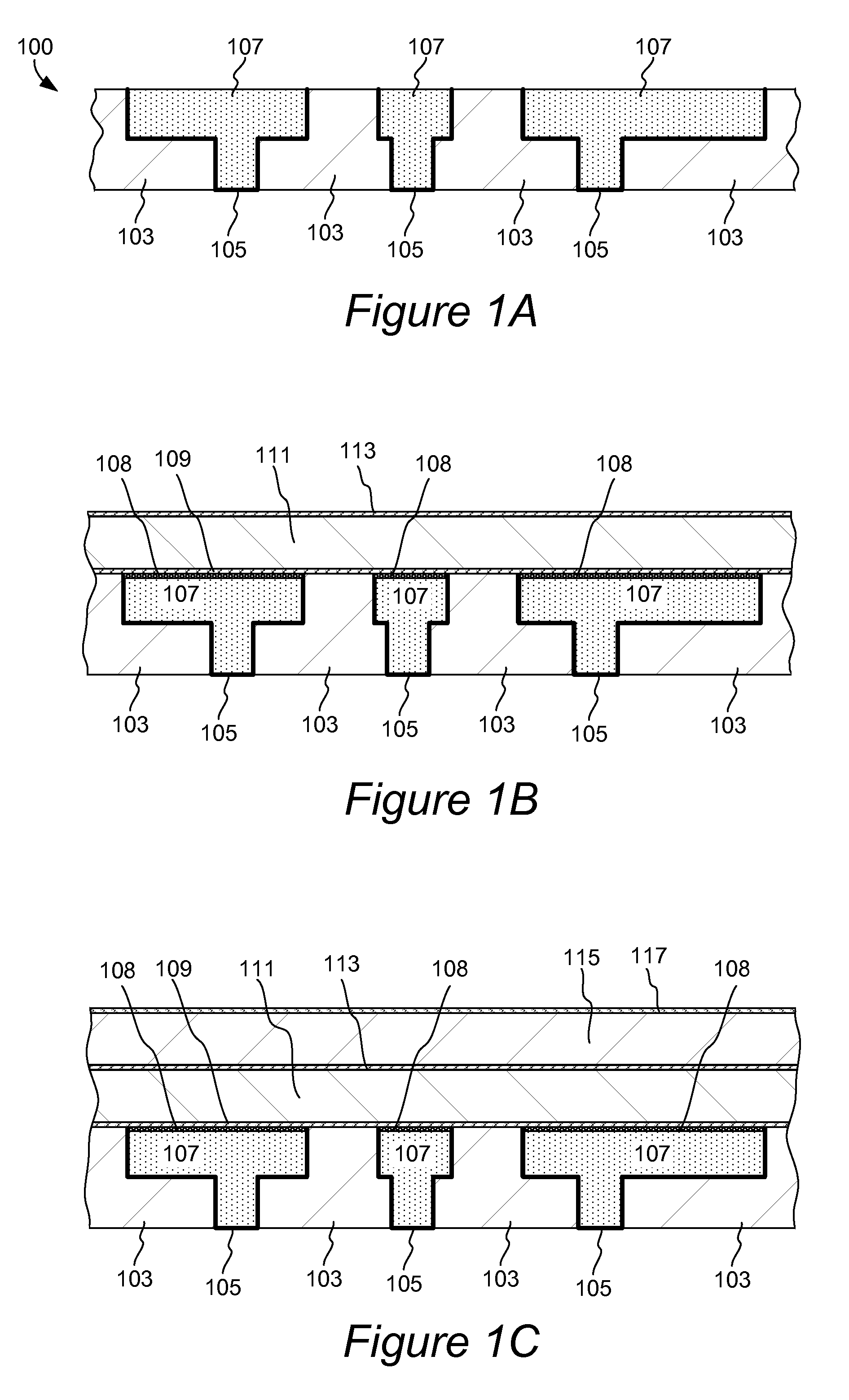
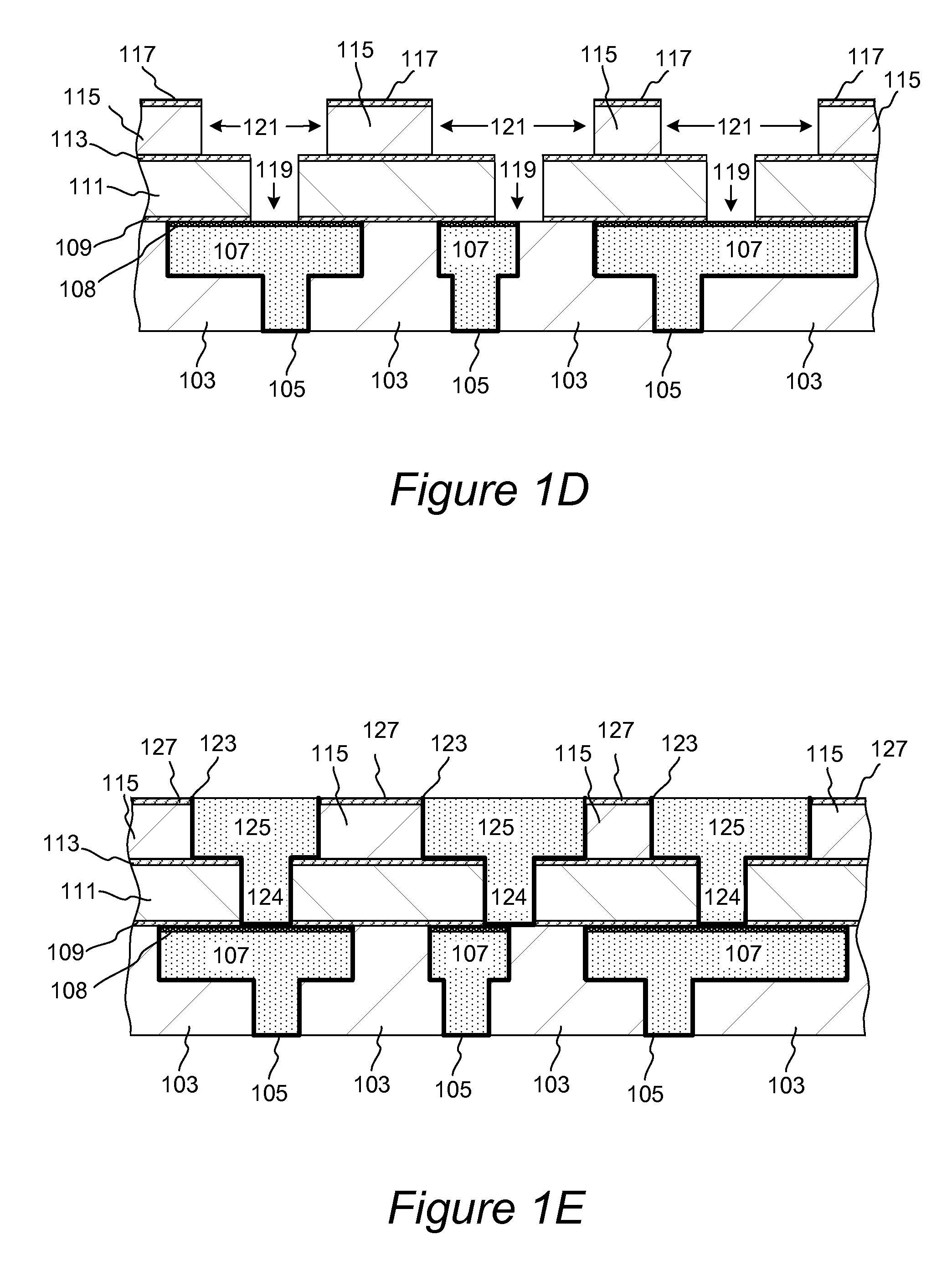
[0006]To address these needs, IC devices having interconnects with protective self aligned buffer (PSAB) layers are provided. Methods of forming PSAB layers during IC device fabrication are also described herein. PSAB layers are layers of material that are selectively formed at the surface of metal layers of a partially fabricated semiconductor device. PSAB layers may be capable of improving several properties of Damascene interconnects. For example, a PSAB layer may promote improved adhesion between a metal layer and an adjacent dielectric diffusion barrier layer. Further, PSAB layers can protect metal surfaces from inadvertent oxidation during fabrication processes and can lead to a decrease in metal electromigration during end use of a semiconductor device. Methods of forming PSAB-containing interconnects having reduced stress migration parameters are also provided.
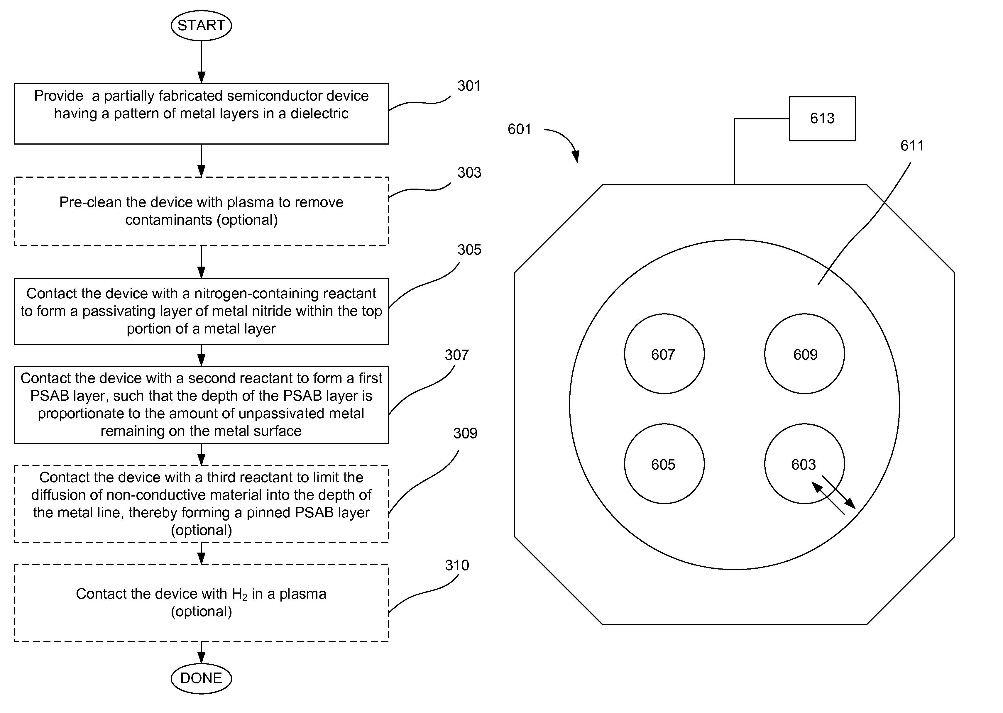
[0007]In some embodiments, a PSAB layer is formed entirely within the top portion of a metal layer, such that it is substantially at the same level as the plane of a dielectric field region adjacent to the metal layer. This can be accomplished by chemically transforming exposed metal atoms to a desired material. For example, Cu can react with SiH4 to form a thin PSAB layer of CuxSiy within the top portion of metal layer. While PSAB layers generally increase resistance of interconnects, such resistance shift can be efficiently controlled. Specifically, thickness of PSAB layers, and, consequently, resistance of an interconnect can be controlled by partially passivating exposed metal surfaces, prior to formation of the PSAB layer. Such passivation can be accomplished by, for example, controllably reacting surface atoms with a nitrogen-containing compound (e.g., NH3) to form a metal nitride. Such passivation depletes the amount of metal atoms (in a zero oxidation state) that are available for reaction to form the PSAB layer, and, consequently, controls the thickness of the PSAB layer and resistance of an interconnect.
[0011]In some embodiments, the first PSAB layer resides entirely within the metal layer. The depth of the first PSAB layer is regulated by an amount of the passivated material (e.g., metal nitride) formed in the first operation, and can range, for example, between 10-1000 Å. The greater the amount of the passivated material formed at the metal surface, the less is the depth of the first PSAB layer. Thus, the thickness of the first PSAB layer, and, consequently, resistance of interconnect, is controlled via a partial passivation of exposed metal surface. In certain embodiments, PSAB layers having a thickness ranging between about 10-60 Å can be formed in a controlled fashion. Control can be achieved, in some embodiments, by regulating the contact time of the nitrogen containing passivating reagent with the substrate.
[0017]In some embodiments, the first formed PSAB layer may be further treated to form a so-called “pinned” PSAB layer. “Pinning” is often used to chemically transform intermediates and by-products generated during formation of the first PSAB layer to materials that do not readily diffuse into the depth of metal lines. Thus, pinning, controls interconnect resistance by limiting diffusion of non-conducting species into metal-filled vias and trenches. In some embodiments, pinning can also partially or completely chemically transform the material of the first PSAB layer. Certain pinning reagents, such as hydrocarbons, form pinned PSAB layers that result in improved stress migration performance of formed interconnects.
[0023]In another aspect, a method of forming a PSAB layer of material includes contacting the partially fabricated semiconductor device with a PSAB forming reactant to form a first PSAB layer, followed by a pinning operation, which comprises contacting the first PSAB layer with a pinning process gas in a plasma and contacting the device with H2 in a plasma. H2 plasma treatment can be performed concurrently with the pinning operation or subsequent to pinning, as a post-treatment step. Use of H2 plasma treatment as a pinning reactant reduces stress migration in the formed interconnects.
[0024]In another aspect a method of forming a PSAB layer of material includes contacting the partially fabricated semiconductor device with a PSAB forming reactant to form a first PSAB layer, followed by a pinning operation, which comprises contacting the first PSAB layer with a process gas comprising a hydrocarbon to form a pinned PSAB layer. Use of hydrocarbon as a pinning reactant reduces stress migration in the formed interconnects.

Problems solved by technology

Further, PSAB layers can protect metal surfaces from inadvertent oxidation during fabrication processes and can lead to a decrease in metal electromigration during end use of a semiconductor device.

Method used


Image

  • Protective self-aligned buffer layers for damascene interconnects
  • Protective self-aligned buffer layers for damascene interconnects
  • Protective self-aligned buffer layers for damascene interconnects

Examples


examples

[0114]One example of a PSAB-forming process is illustrated in an experimental timing diagram shown in FIG. 8. Flow rates of process gas components and plasma parameters are plotted as a function of time. X-axis lists process time in seconds, and Y-axis lists arbitrary parameters that correlate with flow rates and plasma power. Curve (a) corresponds to H2 flow, curve (b) to NH3 flow, and curve (c) to SiH4 flow. Curve (d) corresponds to HF RF power level, and curve (e) to LF RF power level.

[0115]In the described example, the process is started by a plasma pre-clean operation. The partially fabricated semiconductor device having an exposed pattern of copper lines in a dielectric was obtained after a CMP operation, and was placed into a process chamber of a PECVD VECTOR™ apparatus. The entire PSAB-forming process was performed at one station of a four-station apparatus. First, the substrate was pre-heated to 275° C., and H2 was introduced into the process chamber at a flow rate of 4000 ...


PUM

PropertyMeasurementUnit
temperatureaaaaaaaaaa

Abstract

Protective self aligned buffer (PSAB) layers are layers of material that are selectively formed at the surface of metal layers in a partially fabricated semiconductor device. In a Damascene interconnect, PSAB layer typically resides at an interface between the metal layer and a dielectric diffusion barrier layer. PSAB layers promote improved adhesion between a metal layer and an adjacent dielectric diffusion barrier layer. Further, PSAB layers can protect metal surfaces from inadvertent oxidation during fabrication process. A PSAB layer may be formed entirely within the top portion of a metal layer, by, for example, chemically converting metal surface to a thin layer of metal silicide. Thickness of PSAB layers, and, consequently resistance of interconnects can be controlled by partially passivating metal surface prior to formation of PSAB layer. Such passivation can be accomplished by controllably treating metal surface with a nitrogen-containing compound to convert metal to metal nitride.

Description

CROSS-REFERENCE TO RELATED APPLICATIONS[0001]This application is a division claiming priority from U.S. patent application Ser. No. 11 / 709,293 filed Feb. 20, 2007 (now U.S. Pat. No. 7,727,881, issued on Jun. 1, 2010), titled “Protective Self-Aligned Buffer Layers for Damascene Interconnects”, naming Chattopadhyay et al. as inventors, which is a continuation-in-part claiming priority under 35 USC 120 from U.S. patent application Ser. No. 10 / 980,076 filed Nov. 3, 2004 (now U.S. Pat. No. 7,396,759, issued on Jul. 8, 2008), titled “Protection of Cu Damascene Interconnects by Formation of a Self-aligned Buffer Layer,” naming van Schravendijk et al. as inventors, which are incorporated herein by reference in their entireties for all purposes.FIELD OF THE INVENTION[0002]The present invention pertains to methods of forming layers of material on a partially fabricated integrated circuit. Specifically, the invention pertains to methods for forming protective self-aligned buffer (PSAB) layers ...

Claims


Application Information

Patent Timeline
Patent Type & Authority Patents(United States)
IPC IPC(8): C23F1/00C23C16/00H01L21/306
CPCH01L21/76834H01L21/76846H01L21/76849H01L21/76856H01L21/76862H01L21/76867H01L21/76883H01L21/76886H01L23/53238H01L21/76831H01L2924/0002H01L2924/00
Inventor CHATTOPADHYAY, KAUSHIKVAN SCHRAVENDIJK, BART
Owner NOVELLUS SYSTEMS
Learn More