
Micro concentrators elastically coupled with spherical photovoltaic cells

a technology of photovoltaic cells and concentrators, applied in photovoltaics, electrical equipment, semiconductor devices, etc., can solve the problems of high energy cost of the system, arrays are expensive, inefficient, and sometimes unreliable, so as to improve the utilization of expensive semiconductors, avoid overheating, and make arrays expensive. the effect of high efficiency

Inactive Publication Date: 2011-09-06
ENERGY RELATED DEVICES +1
View PDF7 Cites 24 Cited by
  • Summary
  • Abstract
  • Description
  • Claims
  • Application Information

AI Technical Summary

Benefits of technology

[0002]Almost the entire cost of solar arrays is due to the large amount of expensive semiconductor used in current solar cell apparatus. Current solar cell technologies make arrays expensive, inefficient, and sometimes unreliable. Our innovation is a method of mass producing an array of cells with elastic contacts that also concentrate light to better utilize the expensive semiconductor, while not overheating, and reducing efficiency with the effect of efficient heat removal with small discrete photovoltaic cells. Thus, the system semiconductor cost component can be reduced. While if the concentrating optics costs per unit area are significantly lower then that of the semiconductors then the overall cost per unit area of the photovoltaic cell the cost of electric power produced is lowered. We have estimated that due to the far lower cost of micro-optical concentration systems compared to semiconductors, material costs reductions ranging from four to hundreds of times that of current photovoltaic cell costs can be achieved.
[0003]A practical aspect of creating a photovoltaic array of thousands of discrete photodiodes has lead to the challenge of reliably and efficiently making electrical and thermal connections to thousands of discrete semiconductors over a range temperature. We have found that attempts to create long strings of silicone photodiodes mounted on plastic substrates resulted in stresses and cracking failures from differential thermal expansion of building up in the assembly. In this patent elastic electrical and thermal contacts are used to hold the semiconductor bodies in place and allow the assembled system to flex and go through wide ranges of temperature change without losing contact or mechanical disassembly between dissimilar materials with a range of temperature coefficients. The geometry of periodically changing the direction of the electrical contacts and circuits on a substrate can also be used to avoid accumulating yield stress in electrical contacts due to differential thermal expansion or flexure of the system. Thereby keeping the electrical contacts in the elastic regime. Electrical contacts may be welded or soldered together while still maintaining the elastic compression on the solder or weld points prevents the electrical contacts from achieving yielding stresses in the soldered or weld points due to thermal expansion and mechanical vibrations. The elastic contacts make it possible to assemble the arrays with wide tolerances in the construction of the components.
[0004]The micro-concentration, efficient, and heat-sinking concept comes from the simple observation that smaller optics such as raindrops on leaves can concentrate sunlight hundreds of times into small spots without thermally burning the leaves. By concentrating sunlight, the solar cells can be run more efficiently and more cost effectively using the expensive semiconductor materials to transform them into a practical device photovoltaic array that can be produced as discrete cells, electrical connections, and mated with micro concentrating mirrors and lenses (U.S. Pat. No. 5,482,568). We have built several concentrator systems that test the concept. A solar concentrator system using a 2 cm diameter cylindrical glass rod, a sheet aluminum back reflector, and a 2 mm wide crystalline photovoltaic cell achieved seven times increase in the power output compared to the photovoltaic cell without the concentrating optics. There was an insignificant detrimental temperature rise in the photovoltaic cell with the light concentration. In another experiment we have observed that a focused spot from a microscope objective lens with a spot size of 18 microns on a silicone photovoltaic cell achieved an optical concentration of 34,000 suns while experiencing only a 2-degree temperature rise. The performance of the photovoltaic cell only experienced a 3% reduction in performance due to the higher concentration of light into a single spot on the photovoltaic cell. Thus with small dimensional optics, small photovoltaic cell and heat distribution surfaces very high concentrations and in turn high utilization's of the semiconductors can be achieved. The invention of this patent is focused on the practical aspect of forming reliably, and at low cost, the immense number of optical concentrators and individual cells to form practical power systems. The electrical connector can form part of the reflective optics as in our previous U.S. Pat. No. 5,482,568 patent. This electrical interconnection system can also form a reliable network that is tolerant of point failures.

Problems solved by technology

The primary limitation to solar energy is the high cost of the system.
Almost the entire cost of solar arrays is due to the large amount of expensive semiconductor used in current solar cell apparatus.
Current solar cell technologies make arrays expensive, inefficient, and sometimes unreliable.
Our innovation is a method of mass producing an array of cells with elastic contacts that also concentrate light to better utilize the expensive semiconductor, while not overheating, and reducing efficiency with the effect of efficient heat removal with small discrete photovoltaic cells.
A practical aspect of creating a photovoltaic array of thousands of discrete photodiodes has lead to the challenge of reliably and efficiently making electrical and thermal connections to thousands of discrete semiconductors over a range temperature.
We have found that attempts to create long strings of silicone photodiodes mounted on plastic substrates resulted in stresses and cracking failures from differential thermal expansion of building up in the assembly.

Method used


Image

  • Micro concentrators elastically coupled with spherical photovoltaic cells
  • Micro concentrators elastically coupled with spherical photovoltaic cells
  • Micro concentrators elastically coupled with spherical photovoltaic cells

Examples


Embodiment Construction

Description Drawings

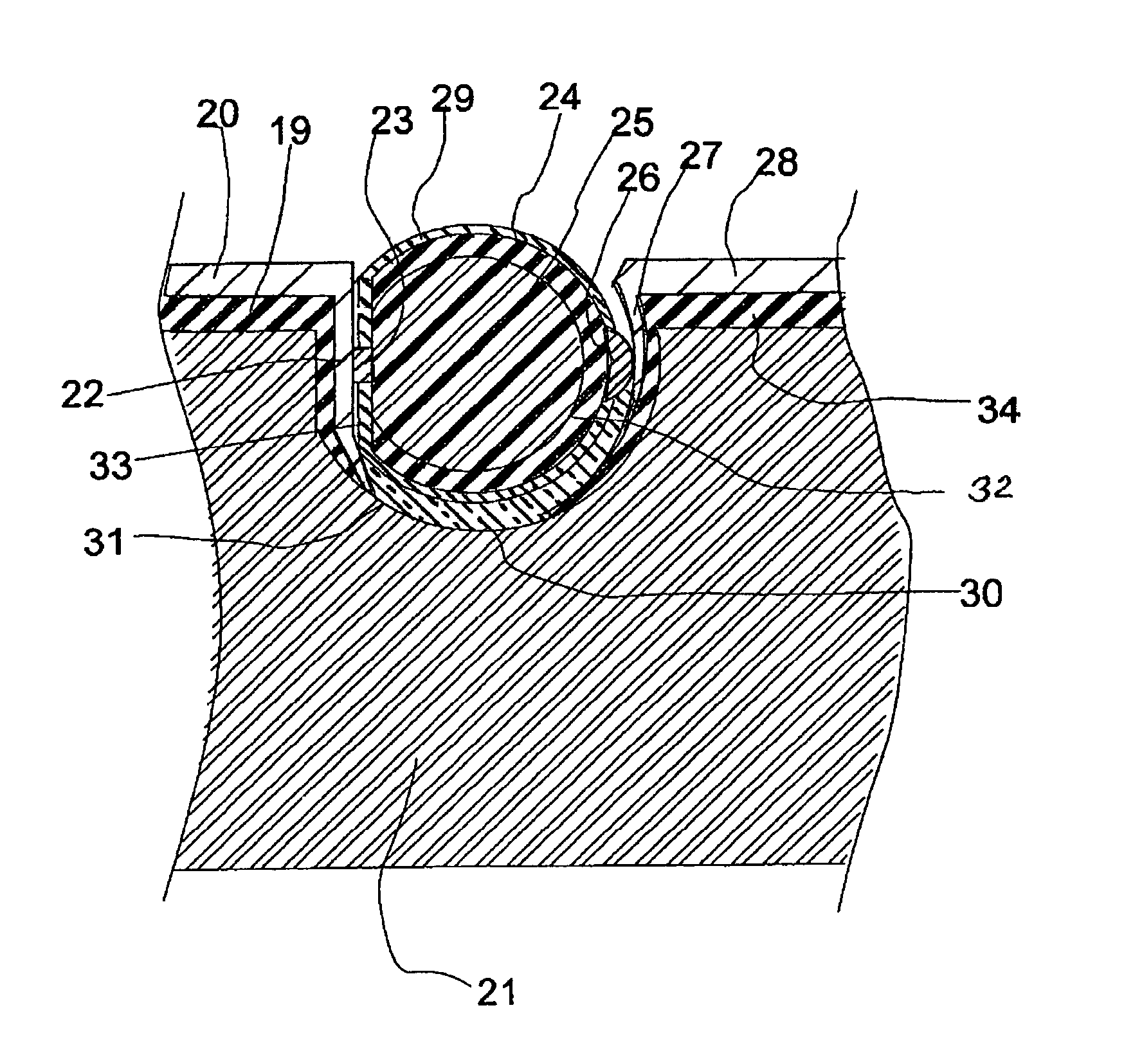
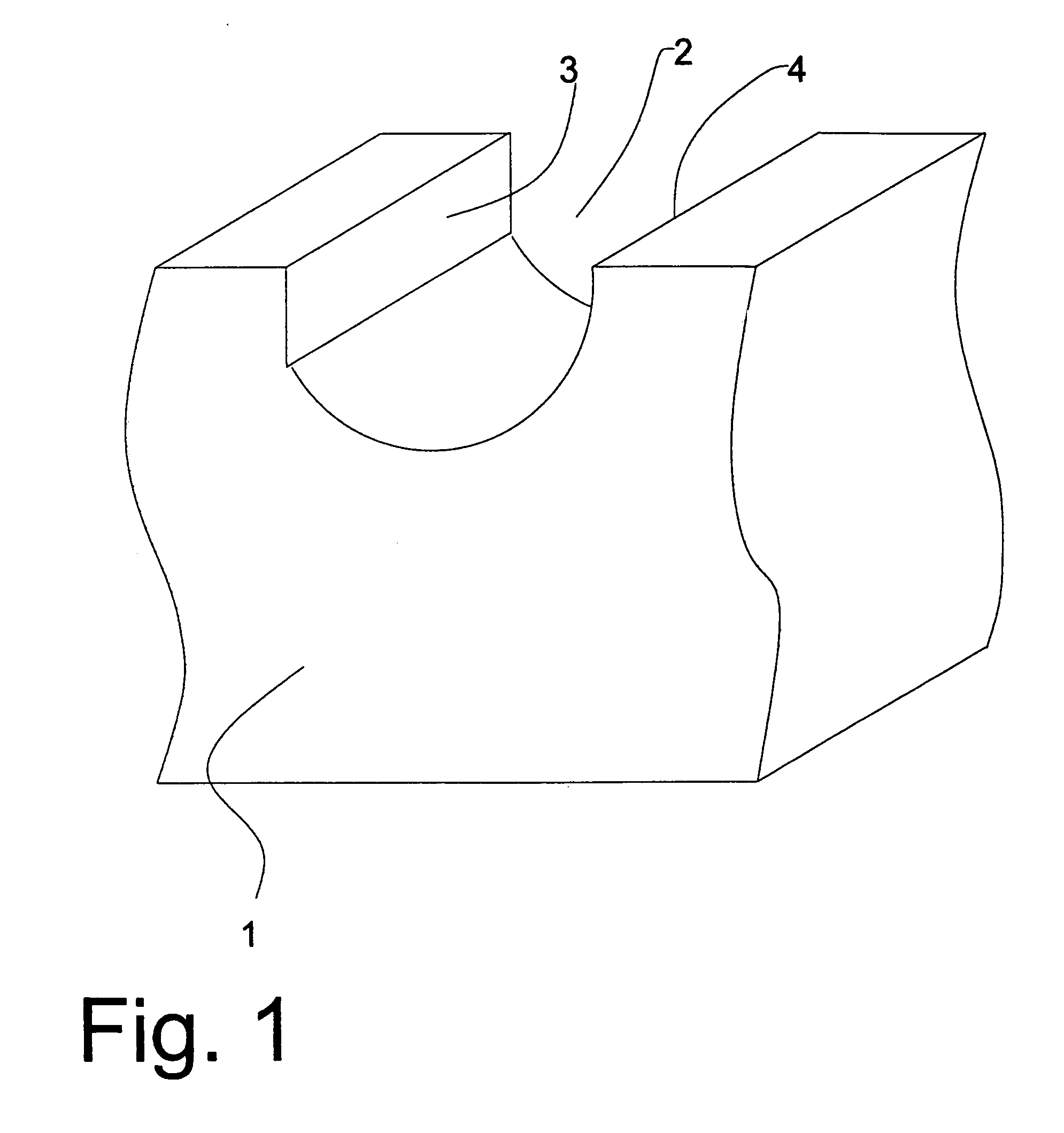
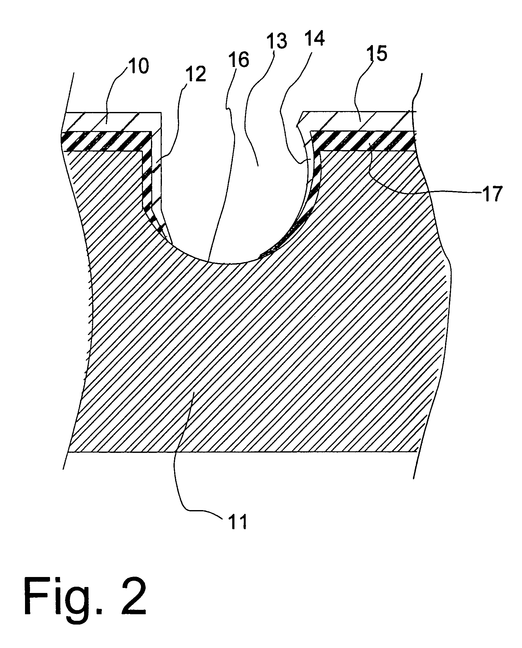
[0261]Several typical embodiments of the invention are illustrated in the following frames. In these drawings several variations in assembly and arrangements will be shown. In FIG. 1 a slot is cut in a dielectric material or molded from a material such as soda lime glass. The glass slot is formed as a flat 3 on one side and curved on the other side 4 to match the curvature of the side grooved semicircular spheres shown later in FIG. 3. The slot 2 may have a slight taper on the flat 3 to accommodate small mounting variations of the semiconductor and assume a tight wedging fit of the semiconductor sphere to the slot 2. Examples of other dielectric materials are:[0262]polyaramid plastic (Asahi-Kasei Chemicals Corporation Co. Ltd. Aramica Division, 1-3-1 Yakoh, Kawaski-Ku, Kawasaki City, Kanagwa 210-0863 Japan).[0263]polyimide plastic, DuPont Films, HPF Customer Services, Wilmington, Del. 19880[0264]silicone rubber, Sylgard® 184 Silicone Optical coupling adhesive Dow...


PUM


Abstract

With small dimensional optics, small photovoltaic cells have heat distribution surfaces, very high concentrations and subsequently high utilization of the semiconductors can be achieved. Discrete photodiodes can be formed as spherical and other geometric shaped, cells with high performance characteristics, precision dimensions, and low cost. This invention positions discrete photovoltaic cells by using their geometric shape, elastic electrical mounts, couples them to small optical concentrator systems of refractory and or reflective optics and makes electrical network connections to those photodiodes, reliably, adjusting for thermal expansion, and at low cost to form low cost and reliable electrical power arrays. The electrical connectors and network can form part of the reflective optics and heat removal system. The electrical interconnection system can also form a reliable network that is self-correcting and tolerant of point failures.

Description

SUMMARY OF THE INVENTION[0001]On a clear sunny day, the sun shines approximately 1,000 Watts of energy per square meter of the planet's surface. Solar energy to electricity conversion has the potential to be an ideal power source solution to escalating energy needs on earth. The primary limitation to solar energy is the high cost of the system. Currently the best photovoltaic cell systems have achieved approximately $2 / Watt, however, to compete with conventional power supplies a factor of four-time reduction of cost, or $0.5 / Watt, needs to be achieved.[0002]Almost the entire cost of solar arrays is due to the large amount of expensive semiconductor used in current solar cell apparatus. Current solar cell technologies make arrays expensive, inefficient, and sometimes unreliable. Our innovation is a method of mass producing an array of cells with elastic contacts that also concentrate light to better utilize the expensive semiconductor, while not overheating, and reducing efficiency w...

Claims


Application Information

Patent Timeline
Patent Type & Authority Patents(United States)
IPC IPC(8): H01L31/042
CPCH01L31/035281H01L31/0543H01L31/0547Y02E10/52
Inventor HOCKADAY, ROBERT G.
Owner ENERGY RELATED DEVICES
Learn More