Simplified switching circuit

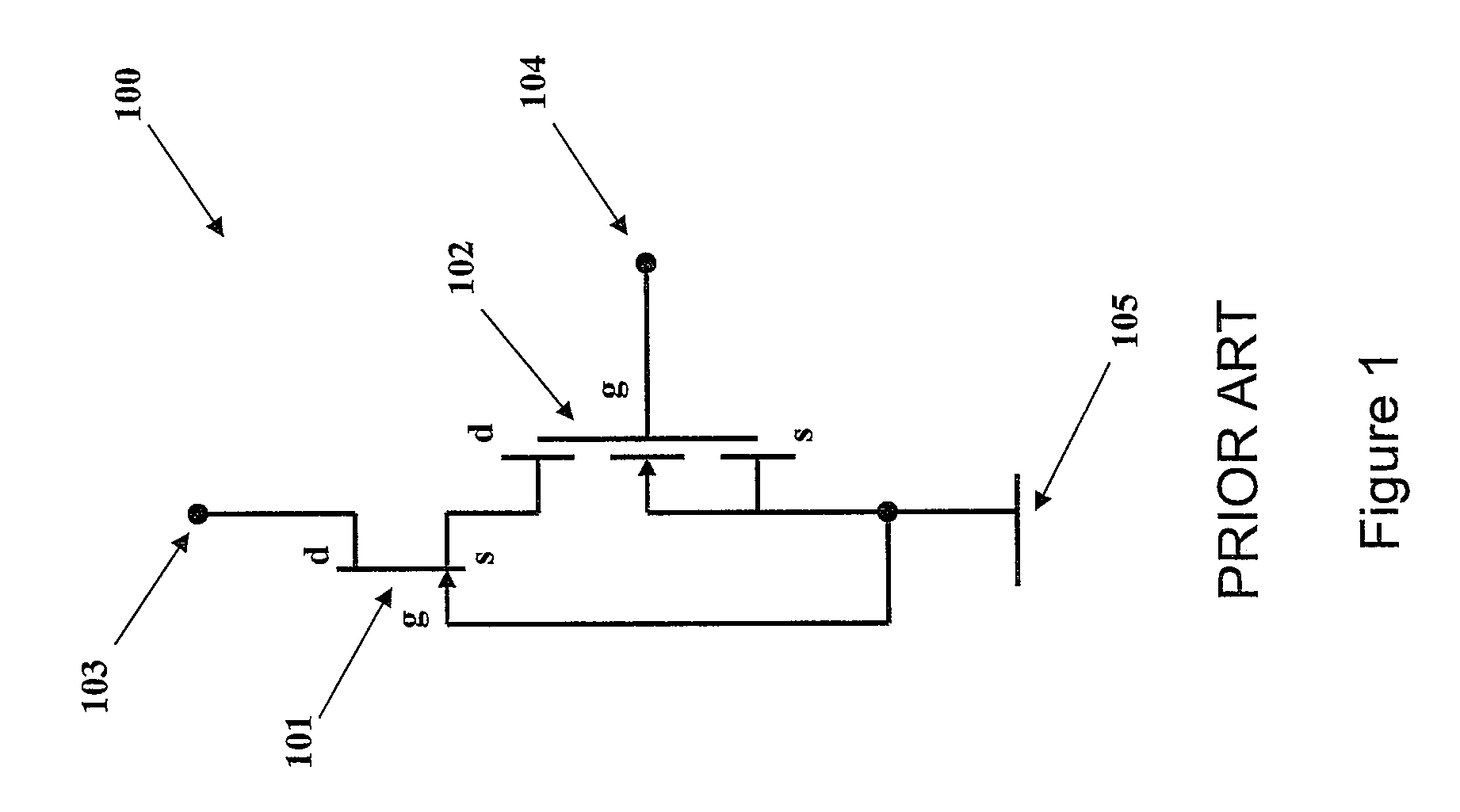
a switching circuit and simplified technology, applied in the direction of electronic switching, pulse technique, electric apparatus, etc., can solve the problems of difficult application of normal characteristics in power switching applications, and the high-frequency switching characteristics of such cascode circuits are generally substantially inferior to those obtainable with a compound semiconductor device operating alon

Active Publication Date: 2010-08-17
INFINEON TECH AUSTRIA AG
View PDF20 Cites 49 Cited by
  • Summary
  • Abstract
  • Description
  • Claims
  • Application Information

AI Technical Summary

Problems solved by technology

A normally on characteristic is generally difficult to apply in power switching applications due to the short circuit that can be produced when an end product is initially coupled to a power source.
However, high-frequency switching characteristics of such cascode circuits are generally substantially inferior to those obtainable with a compound semiconductor device operating alone.

Method used


Image

  • Simplified switching circuit
  • Simplified switching circuit
  • Simplified switching circuit

Examples


Embodiment Construction

[0011]The making and using of the presently preferred embodiments are discussed in detail below. It should be appreciated, however, that the present invention provides many applicable inventive concepts that can be embodied in a wide variety of specific contexts. The specific embodiments discussed are merely illustrative of specific ways to make and use the invention, and do not limit the scope of the invention.

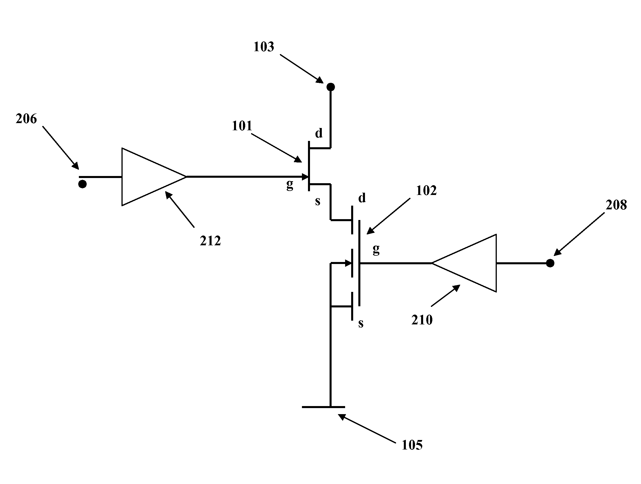
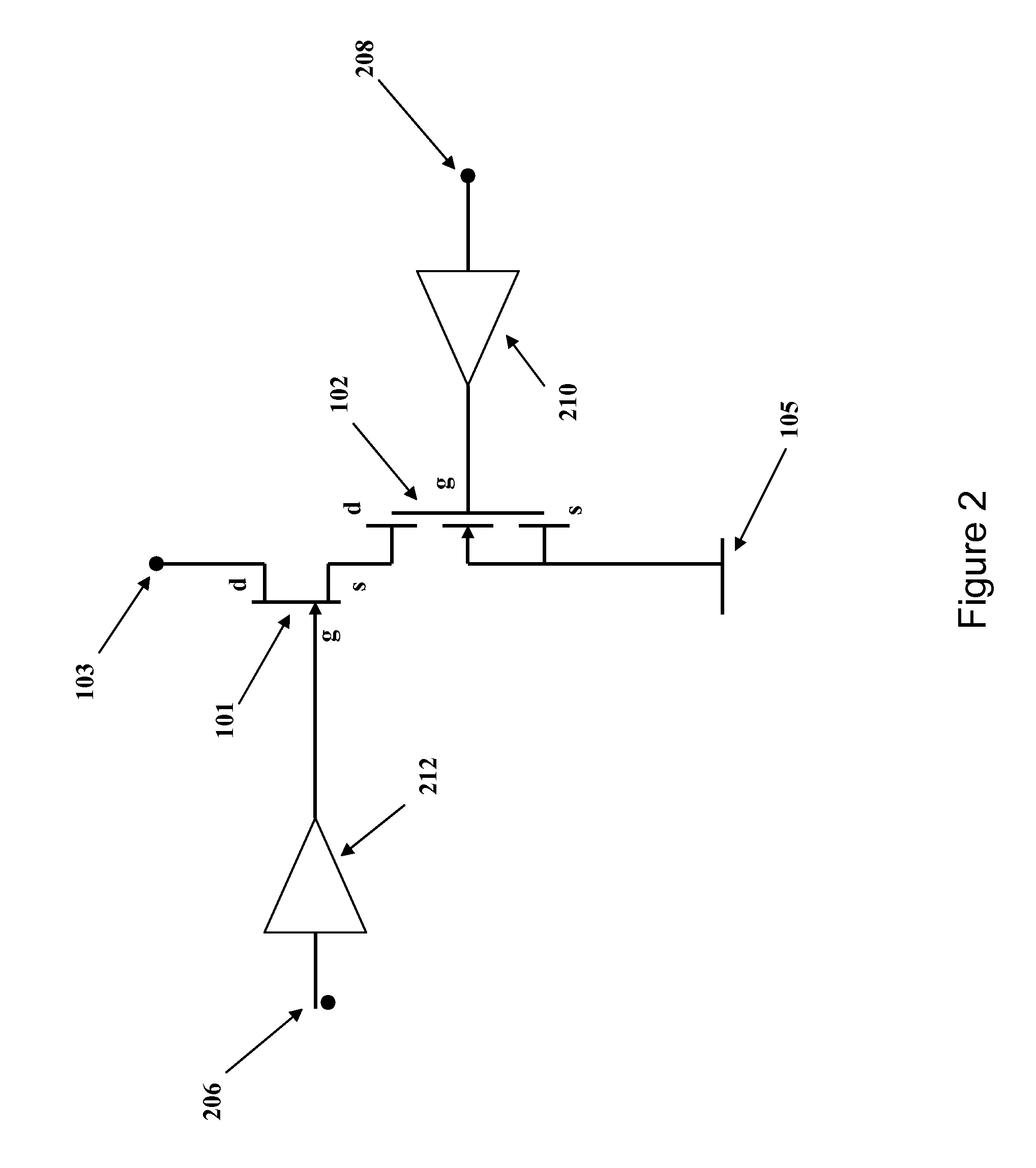
[0012]The present invention will be described with respect to exemplary embodiments in a specific context, namely a switching system formed with a controller that controls the gates of a cascode arrangement of semiconductor devices, the current paths of which are coupled in series, wherein one of the semiconductor devices is an enhancement-mode device, and the other, a depletion-mode device.

[0013]An embodiment of the invention may be applied to various power-switching arrangements, for example, to a power system including a power converter. Other power switching arrangements ...


PUM


Abstract

An embodiment of the invention relates to a switching system that includes a depletion-mode semiconductor device, such as a silicon carbide device, coupled in series with an enhancement-mode semiconductor device, such as a silicon field effect transistor, so that a controller can be configured to disable conductivity of the series arrangement of the two switches during a transient operating condition. During normal high-frequency switching operation, the controller persistently enables the enhancement-mode device to conduct while intermittently enabling the depletion-mode device to conduct. The controller disables the enhancement-mode device to conduct during a transient operating condition such as start up or during a fault, thereby providing circuit protection during such transients. The switching system preserves low loss switching characteristics of the depletion-mode device in a high-frequency switching circuit.

Description

TECHNICAL FIELD[0001]An embodiment of the invention relates generally to semiconductor switching devices and methods, and more particularly to controlling a normally “on” semiconductor device in a circuit that requires a blocking device during startup or during other transient operating conditions.BACKGROUND[0002]Semiconductor devices designed for high-frequency and high-voltage switching applications, particularly those designed for pulse-width controlled power conversion, are increasingly designed with compound semiconductor materials such as silicon carbide. These materials exhibit a wide bandgap between valence and conduction bands, and reasonably high mobility for free carriers. In addition, they can withstand a high internal electric field without breakdown, such as an electric field greater then 106 volts per centimeter (“cm”) that can be sustained in silicon carbide. The result is a device with excellent switching, voltage blocking, and conduction properties in high-power ap...

Claims


Application Information

Patent Timeline
Patent Type & Authority Patents(United States)
IPC IPC(8): H03K17/687
CPCH03K17/567H03K17/6871
Inventor FRIEDRICHS, PETER
Owner INFINEON TECH AUSTRIA AG
Why Eureka
Try Eureka