Eureka AIR delivers breakthrough ideas for toughest innovation challenges, trusted by R&D personnel around the world.

Optoelectronic integrated circuit device and communications equipment using same

a technology of integrated circuits and communications equipment, applied in the direction of instruments, optical elements, optical waveguide light guides, etc., can solve the problems of increasing the number of wires required for transmission, and the crosstalk between wires will become more serious, so as to simplify the routing

Inactive Publication Date: 2010-02-02
RESONAC CORPORATION
View PDF6 Cites 12 Cited by
  • Summary
  • Abstract
  • Description
  • Claims
  • Application Information

AI Technical Summary

Benefits of technology

[0025]Thus, the present invention can provide an optoelectronic integrated circuit device that allows simplification of the routing of optical interconnection paths over the board on which the integrated circuit device is mounted, and that has a configuration in which: the photonic devices provided on the same substrate as the LSI are densely arranged along the four sides of the LSI; and the heat generated within the optoelectronic integrated circuit device does not affect (and hence does not degrade) the characteristics of the laser diode or photodetector of each photonic device. The present invention can also provide a communications device using such an optoelectronic integrated circuit device.

Problems solved by technology

In the case of conventional electrical wiring, if communications systems increase in capacity in the future and hence require a communication equipment capable of processing information at a rate on the order of terabits / sec, the above problems of increased number of wires required for transmission and of crosstalk between the wires will become more serious.

Method used


Image

  • Optoelectronic integrated circuit device and communications equipment using same
  • Optoelectronic integrated circuit device and communications equipment using same
  • Optoelectronic integrated circuit device and communications equipment using same

Examples


first embodiment

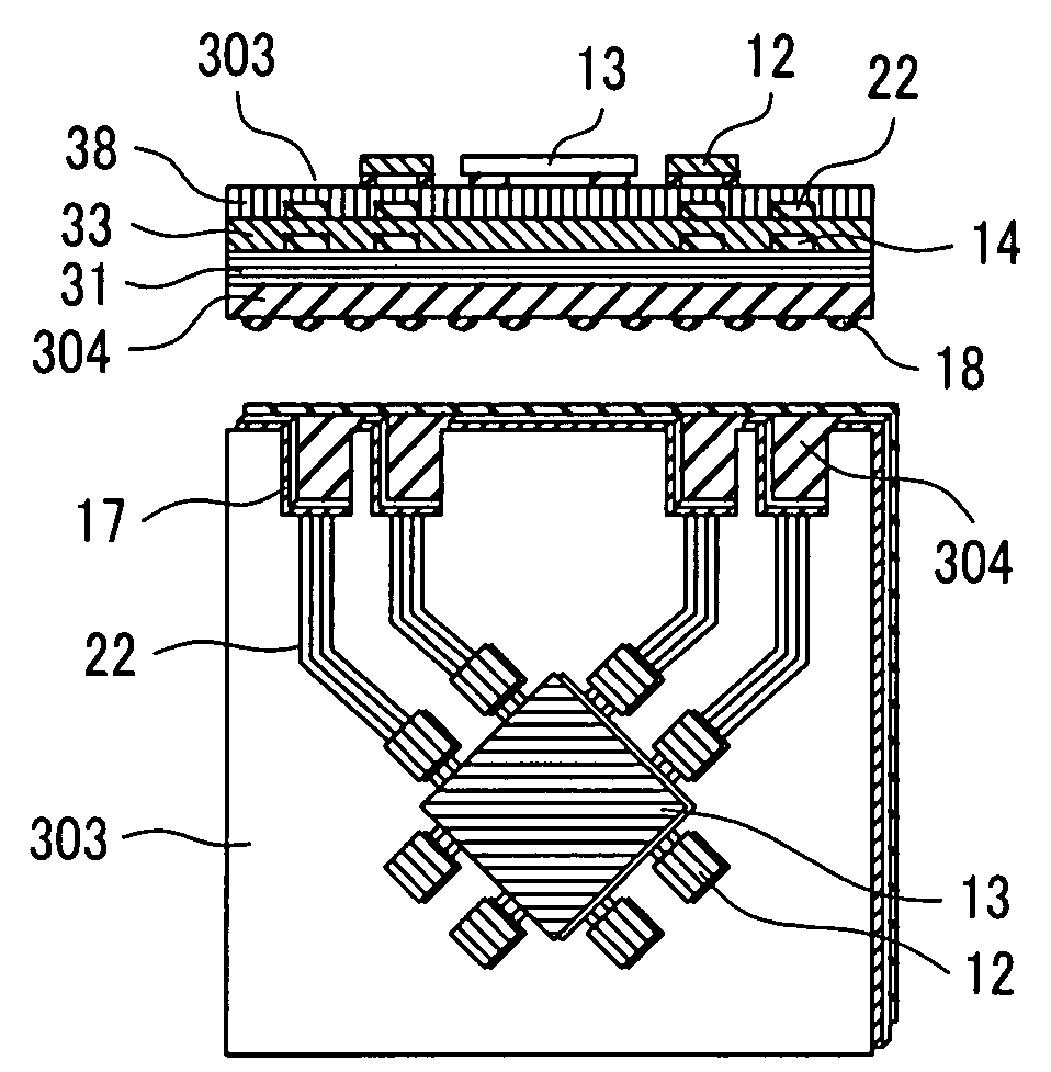
[0027]FIG. 1 is a top view of an optoelectronic integrated circuit device according to a first embodiment of the present invention. In this optoelectronic integrated circuit device, the optical I / O portions of optical waveguides 14 formed on a package substrate 11 are terminated on the same side edge 19 of the substrate 11. FIG. 2 is a cross-sectional view of an optoelectronic integrated circuit device of the first embodiment. As shown in FIG. 2, optical waveguides 22 are formed in a package substrate 21 so as to form two layers. The optical I / O portions of the optical waveguides 22 are terminated on the same side edge of the package substrate. Each optical I / O portion includes a groove 17 in which an optical connector 15 is mounted. Optical fibers (from an external component or device) are optically coupled to their respective optical waveguides 22 through these optical connectors 15. Further, a mirror portion 29 is formed at the other end of each optical waveguide 22, and the ligh...

second embodiment

[0032]FIG. 8 is a top view of an optoelectronic integrated circuit device according to a second embodiment of the present invention. In this optoelectronic integrated circuit device, the optical I / O portions of some optical waveguides (first optical waveguides) formed on a package substrate 11 are terminated on one of the four side edges of the package substrate 11, and those of the other optical waveguides (second optical waveguides) formed on the package substrate 11 are terminated on an adjacent one of the other side edges of the package substrate 11. More specifically, as shown in FIG. 8, first optical waveguides 14 formed on the package substrate 11 and extending from the optical signal input / output terminals of first photonic devices are terminated at fiber connectors 15 on an optical input / output edge portion 80 of the substrate on the backplane side. Second optical waveguides 22 extending from the optical signal input / output terminals of second photonic devices, on the other...

third embodiment

[0034]FIG. 10 is a top view of an optoelectronic integrated circuit device according to a third embodiment of the present invention. In this optoelectronic integrated circuit device, the optical I / O portions of some optical waveguides (first optical waveguides) formed on a package substrate 11 are terminated on one of the four side edges of the package substrate 11, and those of the other optical waveguides (second optical waveguides) are terminated on another one of the side edges of the package substrate 11 facing the above side edge across the substrate center. More specifically, as shown in FIG. 10, first optical waveguides 14 formed on the package substrate 11 and extending from the optical signal input / output terminals of first photonic devices are terminated at fiber connectors 15 on an optical input / output edge portion 80 of the substrate on the backplane side. Second optical waveguides 22 extending from the optical signal input / output terminals of second photonic devices, o...


PUM


Abstract

A photoelectric integrated circuit device, in which photonic devices provided on the same substrate as the LSI are densely arranged along the four sides of the LSI, and characteristic degradation of the laser diode or photo detector due to heat generation can be prevented, furthermore optical wiring is easily performed on the board. A quadrilateral package substrate 11; an LSI package 13 mounted on the package substrate 11; photonic devices 12 mounted along two or more sides of the LSI package 13; first photonic devices electrically connected to I / O terminals disposed on one side of the LSI package 13; second photonic devices electrically connected to I / O terminals disposed on a different side of the LSI package 13; first optical waveguides for connecting between the optical signal I / O terminals of the first photonic devices and an external component or device; and second optical waveguides for connecting between the optical I / O terminals of the second photonic devices and an external component or device; wherein the first and second optical waveguides are terminated on the same side edge of the package substrate 11.

Description

TECHNICAL FIELD[0001]The present invention relates to an optoelectronic integrated circuit device and a mounting configuration thereof for processing large-capacity optical signals (or high data rate optical signals) collectively transmitted and received between boards within a communications equipment. The present invention also relates to a communications equipment using such an optoelectronic integrated circuit device.BACKGROUND ART[0002]Recently, in the field of information and telecommunications, optical communications infrastructures have been rapidly constructed to allow large amounts of data to be exchanged at high speed using light. To date, fiber-optic networks extending a large distance (several kilometers or more) have been built, such as backbone, metro, and access networks. However, in order to further reduce the delay in the transmission of a large amount of data, it is necessary to employ fiber optics (instead of conventional metallic cables and wires) also for inter...

Claims


Application Information

Patent Timeline
Patent Type & Authority Patents(United States)
IPC IPC(8): G02B6/12H01L33/48
CPCG02B6/42G02B6/4214G02B6/421G02B6/4249G02B6/4292G02B6/43G02B6/12
Inventor MATSUOKA, YASUNOBUSHISHIKURA, MASATO
Owner RESONAC CORPORATION
Why Eureka
Eureka Blog
Learn More