Gate electrode having a capping layer

a gate electrode and capping layer technology, applied in the field of semiconductor structure and manufacturing, can solve the problems of compromising the performance and functionality of electronic devices, and the majority of high-k gate dielectric materials are not compatible with crystalline silicon or polycrystalline silicon (polysilicon) gate electrodes

Active Publication Date: 2009-04-28
INTEL CORP
View PDF10 Cites 5 Cited by
  • Summary
  • Abstract
  • Description
  • Claims
  • Application Information

AI Technical Summary

Benefits of technology

[0019]In one embodiment, when the dielectric layer is formed on the substrate, the dielectric layer is a kinetic product. That is, the dielectric layer is formed using a low energy (e.g., low temperature) process. A capping layer is then formed on the kinetic product dielectric layer to seal the dielectric layer until a subsequent high energy process occurs. A high energy (e.g., high temperature) process, such as, for example, annealing, results in a transformation of the dielectric layer from a kinetic product to a thermodynamic product (i.e., more thermodynamically stable). After the transformation, a replacement gate process may be subsequently performed, because the stack can be exposed to oxygen without risking the disadvantageous effects of oxygen exposure. Deposition of a metal gate electrode over the dielectric layer may follow the removal process.
[0020]As shown in FIG. 1 of the accompanying drawings, the process begins by providing a substrate 10. Any well-known substrate, such as, but not limited to, a monocrystalline silicon may be used. In one embodiment, the substrate 10 is a silicon wafer. The substrate 10 may be formed from other materials, such as, but not limited to, germanium, indium antimonide, lead telluride, indium arsenide, indium phosphide, gallium arsenide, gallium antimonide and the like. The substrate 10 may be a silicon-on-insulator structure.
[0021]With reference back to FIG. 1, the process continues by depositing a dielectric layer 12 on the substrate 10. In one embodiment, the dielectric layer 12 is a gate dielectric layer.
[0022]The dielectric layer 12 is desirably made of a high-k material; that is, the high-k dielectric layer 12 is made of a material having a dielectric constant (k) greater than that of silicon dioxide (e.g., ˜4). Some of the materials that may be used to make the high-k gate dielectric layer 12 include, but are not limited to: hafnium oxide, lanthanum oxide, zirconium oxide, zirconium silicon oxide, titanium oxide, tantalum oxide, barium strontium titanium oxide, barium titanium oxide, strontium titanium oxide, yttrium oxide, aluminum oxide, lead scandium tantalum oxide, lead zinc niobate, and the like.
[0023]In one embodiment, the dielectric layer 12 is sufficiently thick to electrically isolate the substrate from a subsequently formed gate electrode. In one embodiment, the thickness of the dielectric layer 12 is about 5-25 angstroms.
[0024]The dielectric layer 12 may be formed on substrate 10 using any suitable technique including, but not limited to, atomic layer deposition (ALD), thermal oxidation, chemical vapor deposition (CVD) and physical vapor deposition (PVD) processes. In one embodiment, the dielectric layer is formed by an ALD process. In the ALD process, the dielectric layer 12 is formed by exposing the substrate to alternating metal-containing precursors and oxygen-containing precursors until a layer having the desired thickness has been formed. Exemplary metal precursors include hafnium tetrachloride and lanthanum trichloride. An exemplary oxygen-containing precursor is water. In another embodiment, the dielectric layer 12 is formed by depositing a metal layer on the substrate and then thermally oxidizing the metal layer.

Problems solved by technology

Silicon dioxide has been the preferred gate dielectric material; however, additional thinning of silicon dioxide compromises the performance and functionality of the electronic devices (e.g., lost function due to charge leakage).
Most high-k gate dielectric materials however, are not compatible with crystalline silicon or polycrystalline silicon (polysilicon) gate electrodes.

Method used


Image

  • Gate electrode having a capping layer
  • Gate electrode having a capping layer
  • Gate electrode having a capping layer

Examples


Embodiment Construction

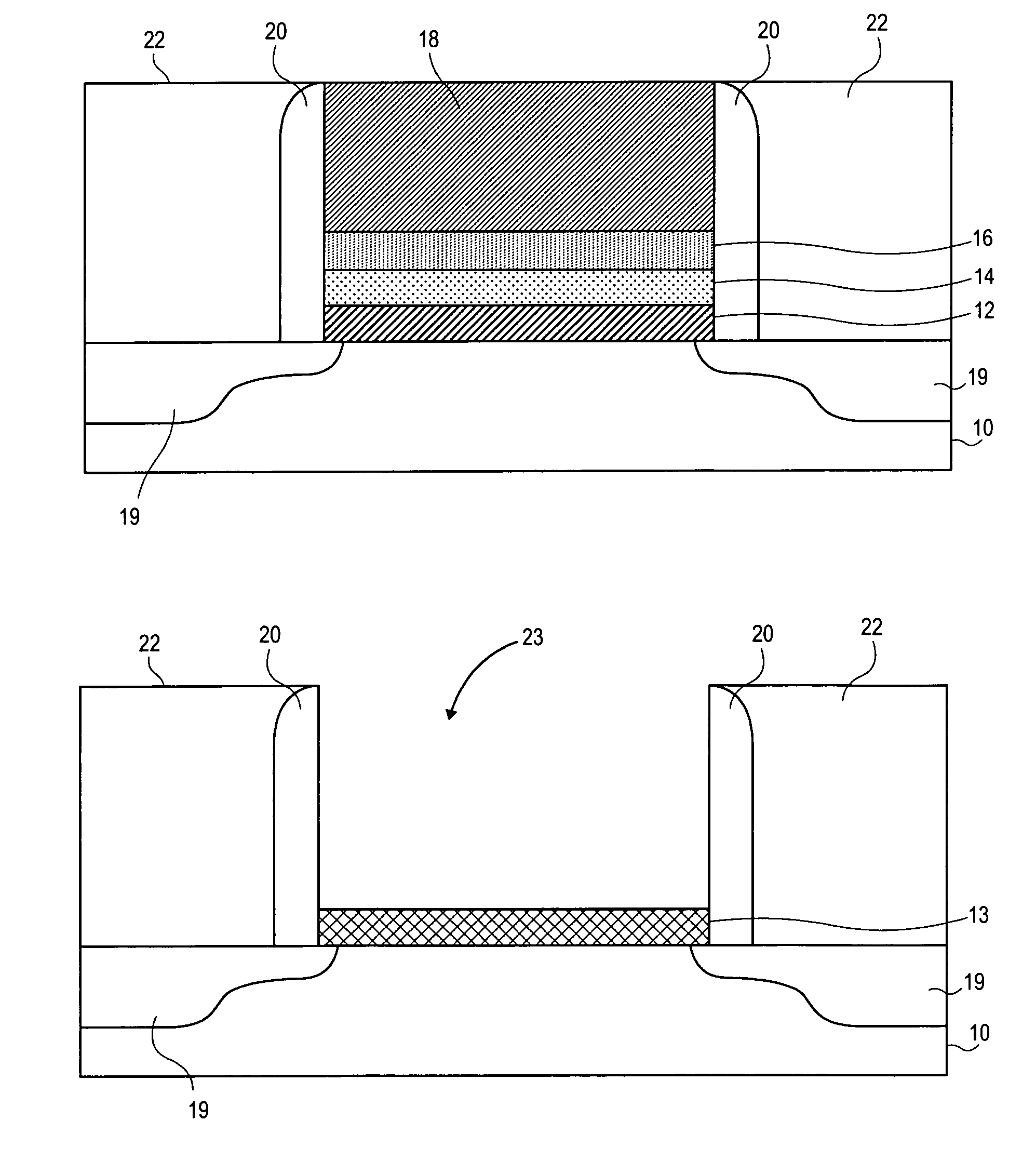
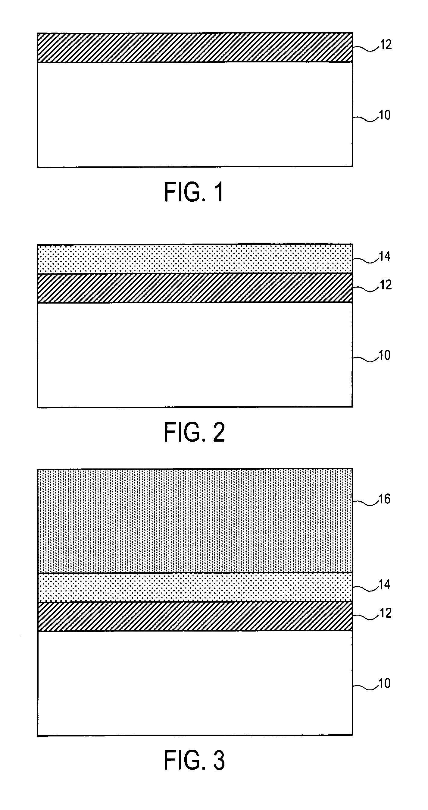
[0018]A method, which includes depositing a dielectric layer on a substrate, followed by deposition of a capping layer in-situ over the dielectric layer prior to any high temperature processing, is disclosed herein. The capping layer acts as an oxygen diffusion barrier or seal to prevent exposure of the dielectric layer to oxygen. An optionally sacrificial barrier layer may be deposited between the dielectric layer and the capping layer. Each of the dielectric layer, barrier layer and capping layer are desirably formed in situ and without exposing the layers to oxygen.

[0019]In one embodiment, when the dielectric layer is formed on the substrate, the dielectric layer is a kinetic product. That is, the dielectric layer is formed using a low energy (e.g., low temperature) process. A capping layer is then formed on the kinetic product dielectric layer to seal the dielectric layer until a subsequent high energy process occurs. A high energy (e.g., high temperature) process, such as, for ...


PUM

PropertyMeasurementUnit
thicknessaaaaaaaaaa
thicknessaaaaaaaaaa
thicknessaaaaaaaaaa

Abstract

A method of manufacturing a semiconductor device and a novel semiconductor device are disclosed herein. An exemplary method includes sputtering a capping layer in-situ on a gate dielectric layer, before any high temperature processing steps are performed.

Description

FIELD OF THE INVENTION[0001]The present invention relates generally to semiconductor structures and manufacturing. In particular, the present invention relates to the manufacturing of high dielectric constant gate stacks.BACKGROUND OF THE INVENTION[0002]Advances in semiconductor manufacturing technology have led to the integration of billions of circuit elements, such as transistors, on a single integrated circuit (IC). In order to integrate increasing numbers of circuit elements onto an integrated circuit it has been necessary to reduce the dimensions of the electronic devices (i.e., a metal-oxide-semiconductor (MOS) transistor).[0003]This scaling down involves making all of the layers in the electronic devices as thin as possible. Silicon dioxide has been the preferred gate dielectric material; however, additional thinning of silicon dioxide compromises the performance and functionality of the electronic devices (e.g., lost function due to charge leakage). One practice has been to...

Claims


Application Information

Patent Timeline
Patent Type & Authority Patents(United States)
IPC IPC(8): H01L21/336
CPCH01L21/28088H01L21/28194H01L21/823828H01L21/823857H01L29/4966H01L29/517H01L29/66545H01L29/78H01L29/513H01L29/665H01L29/6659H01L29/66795H01L21/823437H01L21/823462
Inventor DEWEY, GILBERTDOCZY, MARK L.DATTA, SUMANBRASK, JUSTIN K.METZ, MATTHEW V.
Owner INTEL CORP
Why Eureka
Try Eureka