Multi-chip switch based on proximity communication

a proximity communication and multi-chip technology, applied in the direction of digital storage, instruments, electric digital data processing, etc., can solve the problems of large area occupied by additional circuits, large chip size and complexity, and difficulty in providing interconnections in multi-chip switches

Active Publication Date: 2009-02-10
ORACLE INT CORP
View PDF20 Cites 44 Cited by
  • Summary
  • Abstract
  • Description
  • Claims
  • Application Information

AI Technical Summary

Problems solved by technology

However, high-speed serial ports typically require additional circuits to serialize and deserialize data, to encode and decode data, and to recover an embedded clock.
These additional circuits typically consume a significant amount of the area on an integrated circuit.
These circuits, therefore, may partly determine the size and complexity of a chip.
If the scale of the switch does not allow for a single-chip implementation, the switch may have to be partitioned among several chips with each chip providing a fraction of the aggregate switching capacity.
Unfortunately, it is often challenging to provide interconnects in a multi-chip switch with an aggregate bandwidth that is sufficient to accommodate the total bandwidth of the signals received by the switch.
As a consequence, interconnects in large-scale switches may be complicated and expensive.
Therefore, multi-chip switches often have large footprints and consume significant amounts of power.
Moreover, as the size of a given switch increases, it may be more difficult to control due to increased delays and latency.
This, in turn, may lead to challenges associated with coordinating or scheduling the data flow in the switch.
The complexity and expense associated with the components used to address these challenges can greatly impact the performance and reliability of multi-chip switches.

Method used


Image

  • Multi-chip switch based on proximity communication
  • Multi-chip switch based on proximity communication
  • Multi-chip switch based on proximity communication

Examples


Embodiment Construction

[0042]The following description is presented to enable any person skilled in the art to make and use the invention, and is provided in the context of a particular application and its requirements. Various modifications to the disclosed embodiments will be readily apparent to those skilled in the art, and the general principles defined herein may be applied to other embodiments and applications without departing from the spirit and scope of the present invention. Thus, the present invention is not intended to be limited to the embodiments shown, but is to be accorded the widest scope consistent with the principles and features disclosed herein.

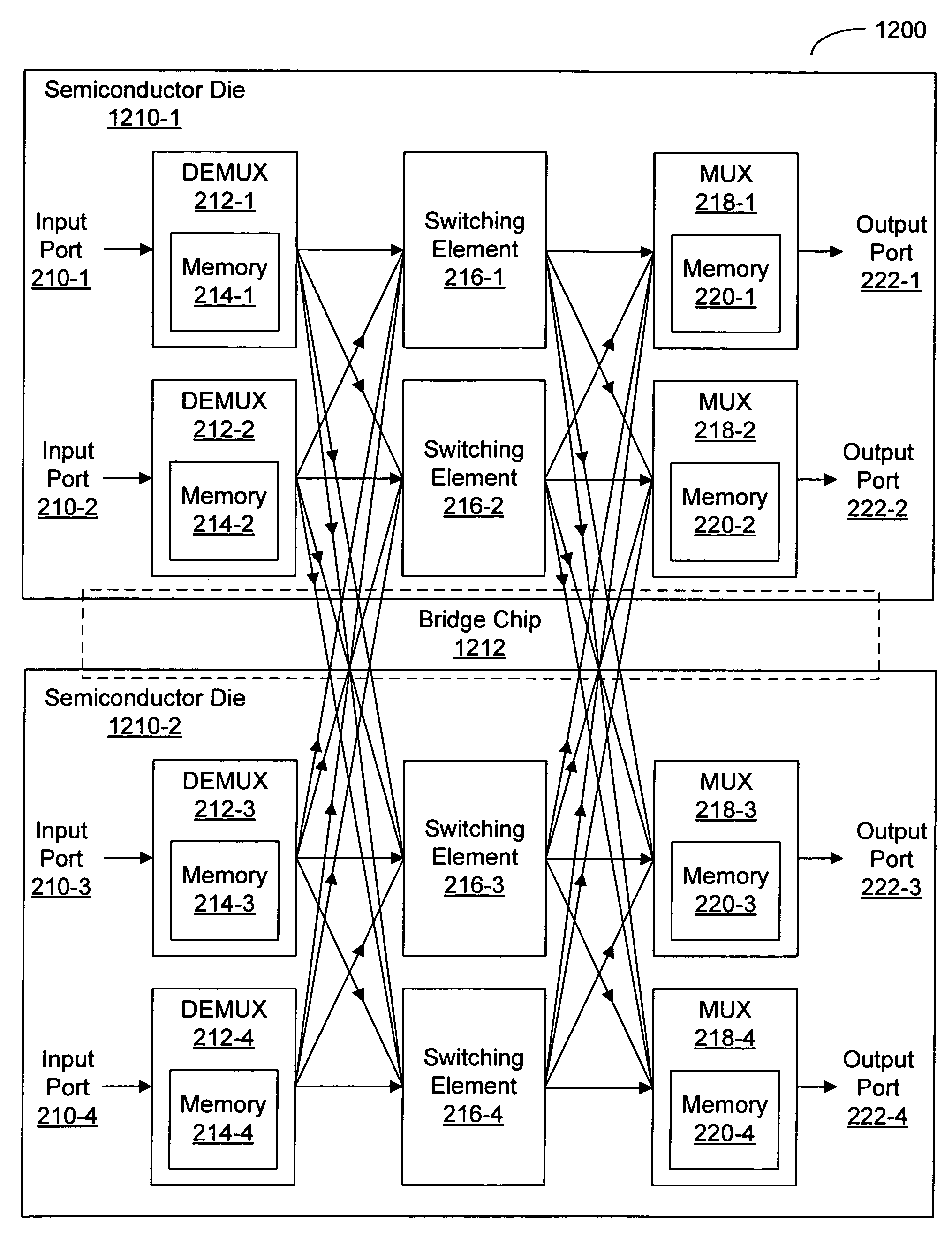
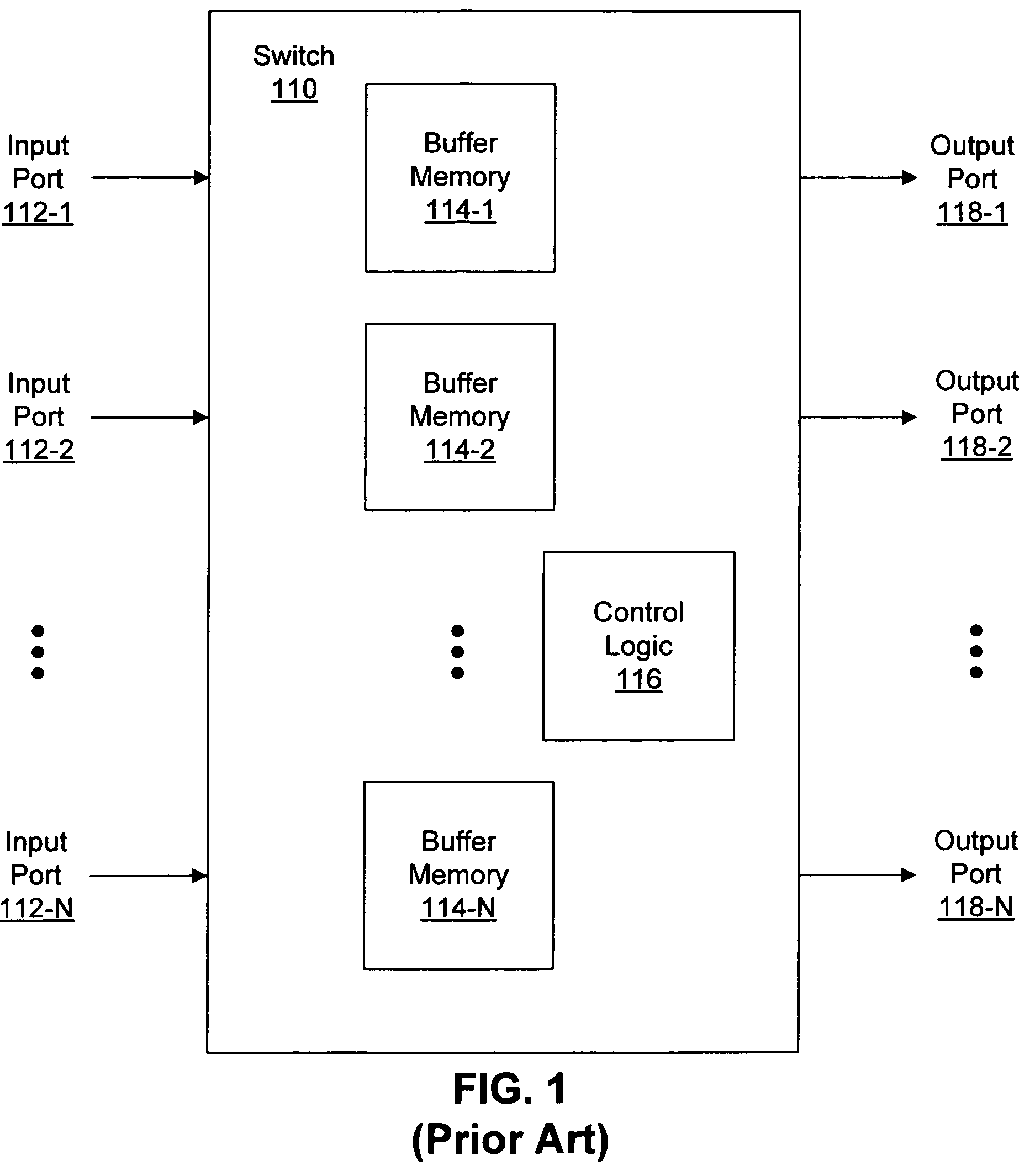
[0043]Embodiments of a method, a switch, and systems that include the switch are described. A semiconductor die in the switch communicates with other semiconductor dies and / or devices in the switch using proximity communication. In proximity communication, a first component (such as a semiconductor die or chip) is situated face-to-face with ano...


PUM


Abstract

A switch contains a first semiconductor die, which is configured to receive signals on a plurality of input ports and to output the signals on a plurality of output ports. The first semiconductor die is further configured to selectively couple the signals between the input and output ports using a plurality of switching elements in accordance with a set of control signals, which correspond to a configuration of the switch. During this process, a plurality of proximity connectors, proximate to a surface of the semiconductor die, are configured to communicate the signals by capacitive coupling.

Description

BACKGROUND[0001]1. Field of the Invention[0002]The present invention relates to techniques for communicating signals through switches. More specifically, the present invention relates to the design of a multi-chip switch comprised of semiconductor dies that communicate with each other using capacitively coupled proximity pads or connectors.[0003]2. Related Art[0004]Many computer systems and networks include switches to selectively communicate data items between different system components. These switches often include multiple input ports and multiple output ports, which are often implemented as high-speed serial input / output (I / O) ports. In contrast with lower-speed parallel ports, these high-speed serial ports offer advantages, such as a reduction in overall power consumption and in associated port area (in terms of the number of printed circuit boards, integrated circuit or chip packages, and / or I / O connectors). However, high-speed serial ports typically require additional circui...

Claims


Application Information

Patent Timeline
Patent Type & Authority Patents(United States)
IPC IPC(8): H05K7/00G06F13/00
CPCH04L49/109H04L49/15H04L49/1515H04L49/254H04L49/3018H04L49/3027
Inventor EBERLE, HANSGURA, NILSOLESINSKI, WLADYSLAW
Owner ORACLE INT CORP
Why Eureka
Try Eureka