
Organic electroluminescent compound, a plurality of host materials, and organic electroluminescent device comprising the same

Pending Publication Date: 2021-10-28
ROHM & HAAS ELECTRONIC MATERIALS LLC
View PDF2 Cites 0 Cited by
  • Summary
  • Abstract
  • Description
  • Claims
  • Application Information

AI Technical Summary

Benefits of technology

[0018]By comprising a specific combination of compounds of the present disclosure as host materials, it is possible to provide an organic electroluminescent device having higher luminous efficiency and/or longer lifespan properties as compared with the conventional organic electroluminescent device, and manufacture a display system or a light system using the same.
[0019]Hereinafter, the present disclosure will be described in detail. However, the following description is intended to explain the disclosure, and is not meant in any way to restrict the scope of the disclosure.
[0020]The term “organic electroluminescent material” in the present disclosure means a material that may be used in an organic electroluminescent device, and may comprise at least one compound. The organic electroluminescent material may be comprised in any layer constituting an organic electroluminescent device, as necessary. For example, the organic electroluminescent material may be a hole injection material, a hole transport material, a hole auxiliary material, a light-emitting auxiliary material, an electron blocking material, a light-emitting material (containing host and dopant materials), an electron buffer material, a hole blocking material, an electron transport material, an electron injection material, etc.
[0021]The term “a plurality of organic electroluminescent materials” in the present disclosure means an organic electroluminescent material as a combination of at least two compounds, which may be comprised in any layer constituting an organic electroluminescent device. It may mean both a material before being comprised in an organic electroluminescent device (for example, before vapor deposition) and a material after being comprised in an organic electroluminescent device (for example, after vapor deposition). For example, a plurality of organic electroluminescent materials may be a combination of at least two compounds which may be comprised in at least one of a hole injection layer, a hole transport layer, a hole auxiliary layer, a light-emitting auxiliary layer, an electron blocking layer, a light-emitting layer, an electron buffer layer, a hole blocking layer, an electron transport layer, and an electron injection layer. At least two compounds may be comprised in the same layer or different layers by means of the methods used in the art, for example, may be mixture-evaporated or co-evaporated, or may be individually evaporated.
[0022]The term “a plurality of host materials” in the present disclosure means an organic electroluminescent material as a combination of at least two host materials. It may mean both a material before being comprised in an organic electroluminescent device (for example, before vapor deposition) and a material after being comprised in an organic electroluminescent device (for example, after vapor deposition). A plurality of host materials of the present disclosure may be comprised in any light-emitting layer constituting an organic electroluminescent device. At least two compounds comprised in a plurality of host materials may be comprised together in one light-emitting layer or may respectively be comprised in different light-emitting layers. If at least two host materials are comprised in one layer, for example, they may be mixtur

Problems solved by technology

However, the development of materials for improv

Method used


Image

  • Organic electroluminescent compound, a plurality of host materials, and organic electroluminescent device comprising the same
  • Organic electroluminescent compound, a plurality of host materials, and organic electroluminescent device comprising the same
  • Organic electroluminescent compound, a plurality of host materials, and organic electroluminescent device comprising the same

Examples


Example

Device Examples 1, 2, and 5 to 12: Producing an OLED by Co-Evaporating the First and Second Host Compounds According to the Present Disclosure

[0074]An OLED according to the present disclosure was produced as follows: A transparent electrode indium tin oxide (ITO) thin film (10 Ω / sq) on a glass substrate for an OLED (GEOMATEC CO., LTD., Japan) was subjected to an ultrasonic washing with trichloroethylene, acetone, ethanol and distilled water, sequentially, and then was stored in isopropanol. The ITO substrate was mounted on a substrate holder of a vacuum vapor deposition apparatus. Compound HI-1 was introduced into a cell of the vacuum vapor deposition apparatus, and then the pressure in the chamber of the apparatus was then controlled to 10$ torr. Thereafter, an electric current was applied to the cell to evaporate the above-introduced material, thereby forming a first hole injection layer having a thickness of 80 nm on the ITO substrate. Next, compound HI-2 was introduced into anot...

Example

Device Example 3: Producing an OLED by Mixture-Evaporating the First and Second Host Compounds According to the Present Disclosure

Example

[0075]An OLED was produced in the same manner as in Device Example 2, except that the first host compound and the second host compound described in Table 1 were deposited in one cell rather than in two cells in a vacuum deposition apparatus.


PUM


Abstract

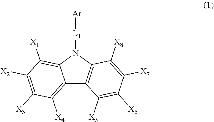
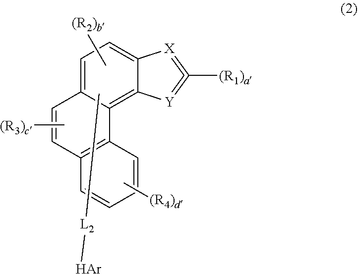
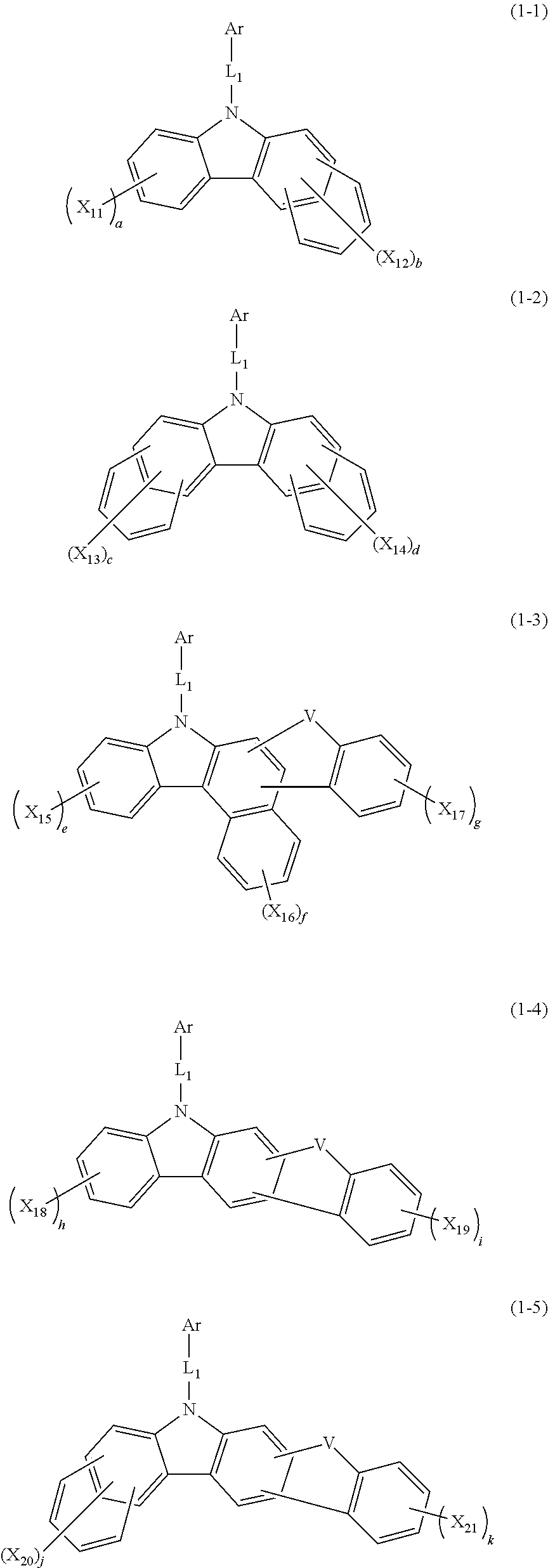
The present disclosure relates to a plurality of host materials comprising a first host material having a compound represented by formula 1, and a second host material having a compound represented by formula 2, and an organic electroluminescent device comprising the same. By comprising a specific combination of compounds of the present disclosure as host materials, it is possible to provide an organic electroluminescent device having higher luminous efficiency and/or longer lifespan properties as compared with a conventional organic electroluminescent device.

Description

TECHNICAL FIELD[0001]The present disclosure relates to a plurality of host materials and an organic electroluminescent device comprising the same.BACKGROUND ART[0002]In 1987, Tang et al. of Eastman Kodak first developed a small molecule green organic electroluminescent device (OLED) of TPD / Alq3 bilayer consisting of a light-emitting layer and a charge transport layer. Since then, the research on an OLED has been rapidly carried out. and it has been commercialized. At present. OLEDs primarily use phosphorescent materials having excellent luminous efficiency in panel implementation. In addition, an OLED having high luminous efficiency and / or long lifespan is required for prolonged use and high resolution of a display.[0003]Korean Patent Appl. Laid-Open No. 2017-0022865 discloses a benzoxazole derivative compound for improving the performance of an OLED. However, the development of materials for improving the performance of an OLED is still required.DISCLOSURE OF THE INVENTIONProblems ...

Claims


Application Information

Patent Timeline
IPC IPC(8): H01L51/00
CPCH01L51/0072H01L51/0073H01L51/5016H01L51/0074H01L51/0067H01L51/0054C07D405/10C07D487/04C07D413/04C07D413/14C09K11/06C07D209/80C07D209/56C07D409/10C07D409/04C07D417/04C07D417/10C07D413/10C07D403/10C07D403/04H10K85/6576H10K85/6574H10K85/657H10K85/342H10K85/6572H10K50/11H10K2101/10H10K2101/90H10K85/622H10K85/654H10K50/12H10K50/15H10K50/171
Inventor KIM, BITNARILEE, SU-HYUNPARK, HYO-SOONHAN, TAE-JUNYANG, JEONG-EUNCHO, SANG-HEEMOON, DOO-HYEON
Owner ROHM & HAAS ELECTRONIC MATERIALS LLC
Learn More