Touch screen display and electronic device including same
a touch screen display and electronic device technology, applied in the direction of instruments, other domestic objects, synthetic resin layered products, etc., to achieve the effect of simplifying the stacking process between the electronic device components, reducing weight, and reducing the weight of electronic devices
- Summary
- Abstract
- Description
- Claims
- Application Information
AI Technical Summary
Benefits of technology
Problems solved by technology
Method used
Image
Examples
first embodiment
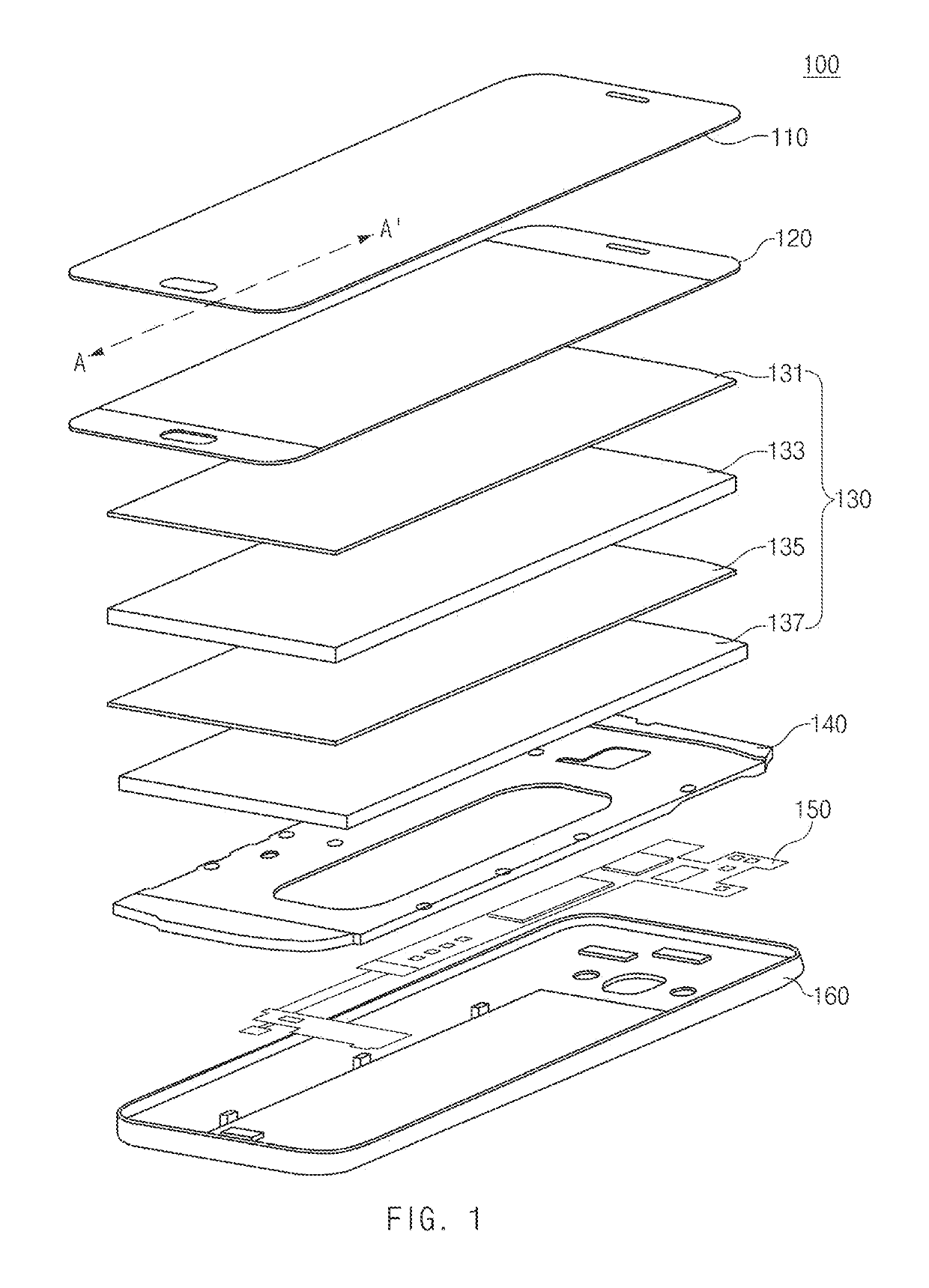
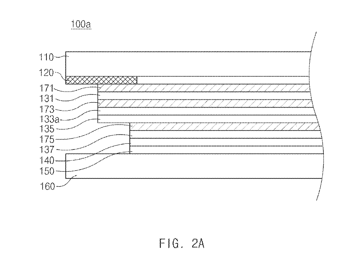
[0049]With reference to FIG. 2A, at least some of components of an electronic device 100a may be stacked in a predetermined order in a first direction (e.g., upper direction side of the support member 140) on the support member 140. For example, the display panel 137, the second polarizing plate 135, a touch panel 133a, the first polarizing plate 131, the cover glass 110 to which the printed member 120 is adhered, and the like may be stacked in order on the top surface of the support member 140.
[0050]With respect to the stacked structure between the components, the photosensitive adhesive member as described above such as photosensitive adhesive members 171, 173, and 175 may be disposed in at least some of spaces between the components. For example, the third photosensitive adhesive member 175, the second photosensitive adhesive member 173, and the first photosensitive adhesive member 171 may be respectively disposed between the display panel 137 and the second polarizing plate 135...
second embodiment
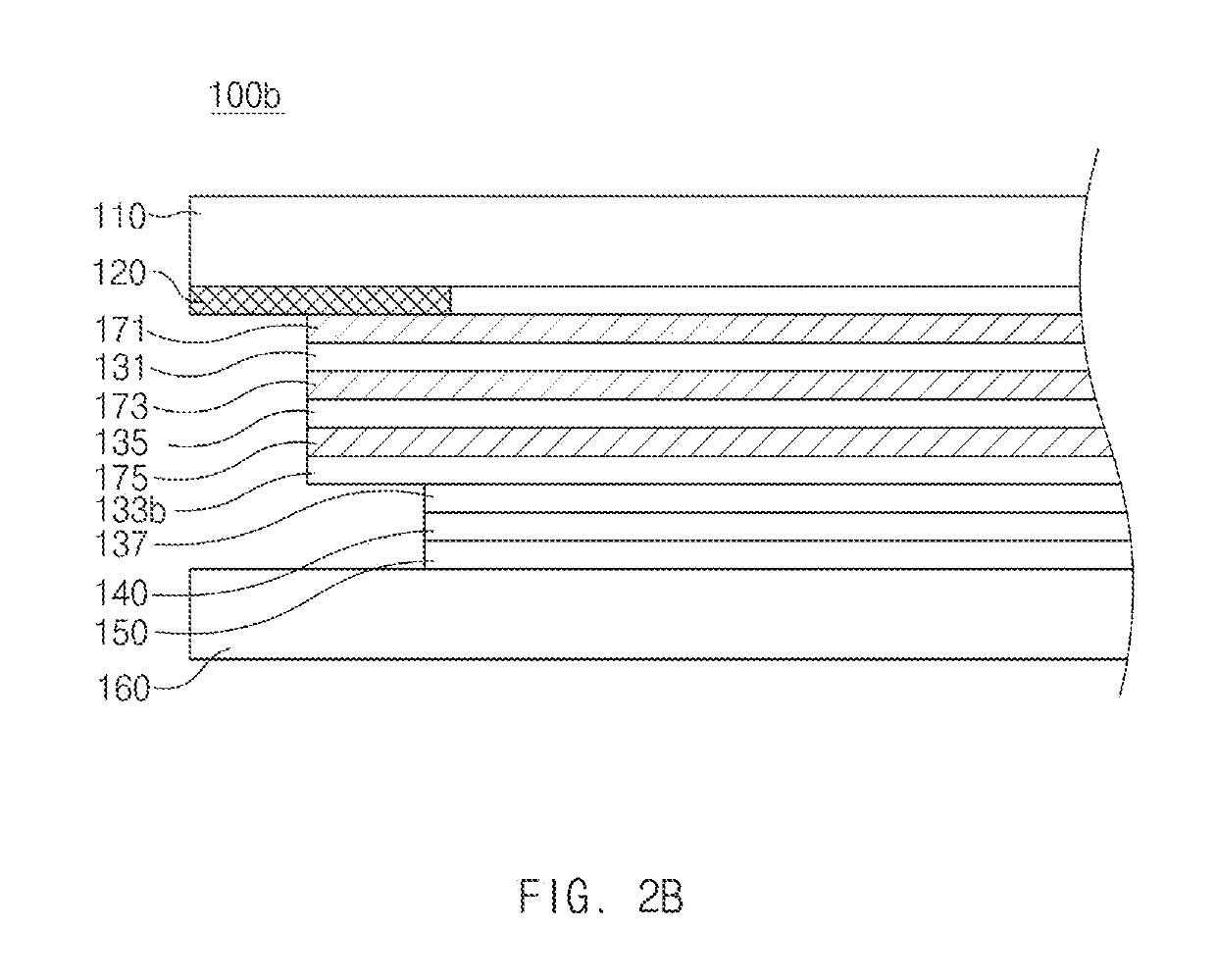
[0056]On the stacked structure of the electronic device 100b the touch panel 133b may be stacked on a top surface of the display panel 137. In this regard, at least some of electrode layers included in the touch panel 133b may be included in the display panel 137. For example, a first electrode layer (e.g., Rx electrode layer) of the touch panel 133b may be mounted on an upper substrate constituting the display panel 137 or formed on the upper substrate (e.g., on-cell mode). Alternatively, the first electrode layer (e.g., Rx electrode layer) and a second electrode layer (e.g., Tx electrode layer) of the touch panel 133b may be formed within the display panel 137 (e.g., in-cell mode). In a case of the in-cell mode, a substrate forming the electrode layer of the touch panel 133b may be excluded, which may contribute to miniaturizing or weight-saving of the electronic device 100b.
[0057]FIGS. 3A to 3C are diagrams illustrating stacking processes between at least some components of an ...
PUM
| Property | Measurement | Unit |
|---|---|---|
| thickness | aaaaa | aaaaa |
| photosensitive | aaaaa | aaaaa |
| flexibility | aaaaa | aaaaa |
Abstract
Description
Claims
Application Information
 - R&D
- Intellectual Property
- Life Sciences
- Materials
- Tech Scout
- Unparalleled Data Quality
- Higher Quality Content
- 60% Fewer Hallucinations
Browse by: Latest US Patents, China's latest patents, Technical Efficacy Thesaurus, Application Domain, Technology Topic, Popular Technical Reports.
© 2025 PatSnap. All rights reserved.Legal|Privacy policy|Modern Slavery Act Transparency Statement|Sitemap|About US| Contact US: help@patsnap.com


