Reactor with heated and textured electrodes and surfaces

a technology of heated and textured electrodes and surfaces, which is applied in the field of reactors, can solve the problems of poor reactor surface adhesion quality, thick deposits or layers, and detrimental effects of various surfaces found in the reactor, and achieves the effects of reducing the number of electrodes, and improving the adhesion quality of the reactor surfa

Inactive Publication Date: 2008-12-25
OEM GROUP INC
View PDF41 Cites 1 Cited by
  • Summary
  • Abstract
  • Description
  • Claims
  • Application Information

AI Technical Summary

Benefits of technology

[0006]Accordingly, it is an object of the invention to provide an apparatus and method which ensures that any layers or deposits on the internal surfaces of the reactor are thin, durable and adhere well to the surface of the reactor so that the deposits do not flake or spauld, potentially interfering with the process of defining the various layers which are being fabricated on a wafer.
[0010]Still a further object of the invention is to provide the reactor with a reactor chamber and surfaces which are textured in order to encourage adherence of materials deposited thereon so that such materials do not flake or spauld off, interfering with the processing of a wafer.
[0012]It is a further object of the present invention to provide a deposition shield which can be at least one of heated and / or textured in order to ensure that any materials deposited thereon adhere to the surface and do not flake or spauld off, potentially interfering with the processing of the substrate.
[0013]It is yet a further aspect of the present invention to coat the internal surfaces of the reactor with adhesion promoters which encourage the development of durable deposits which are less likely to flake or spauld and thus interfere with the processing of the work piece.

Problems solved by technology

The deposits which form on the various surfaces found in the reactor are known to have a detrimental effect to the fabrication of the semiconductor wafer product in the reactor.
By way of example only, such deposits and layers on surfaces of the reactor can be thick and have poor reactor surface adhesion qualities.
Additionally, the deposits or layers may not be very durable.
All this potentially leads to the flaking or spaulding off of portions of the deposits or layers from the surfaces of the reactor.
Such flaking or spaulding can interfere with the uniform processing of the surface of the wafer.
For example, materials which flake or spauld from the surface of a reactor can redeposit on the surface of the wafer being processed, potentially damaging the functionality being fabricated on the wafer.

Method used


Image

  • Reactor with heated and textured electrodes and surfaces
  • Reactor with heated and textured electrodes and surfaces
  • Reactor with heated and textured electrodes and surfaces

Examples


Embodiment Construction

Embodiment with a Heated Upper, Lower and Side Electrodes and Other Heated Surfaces

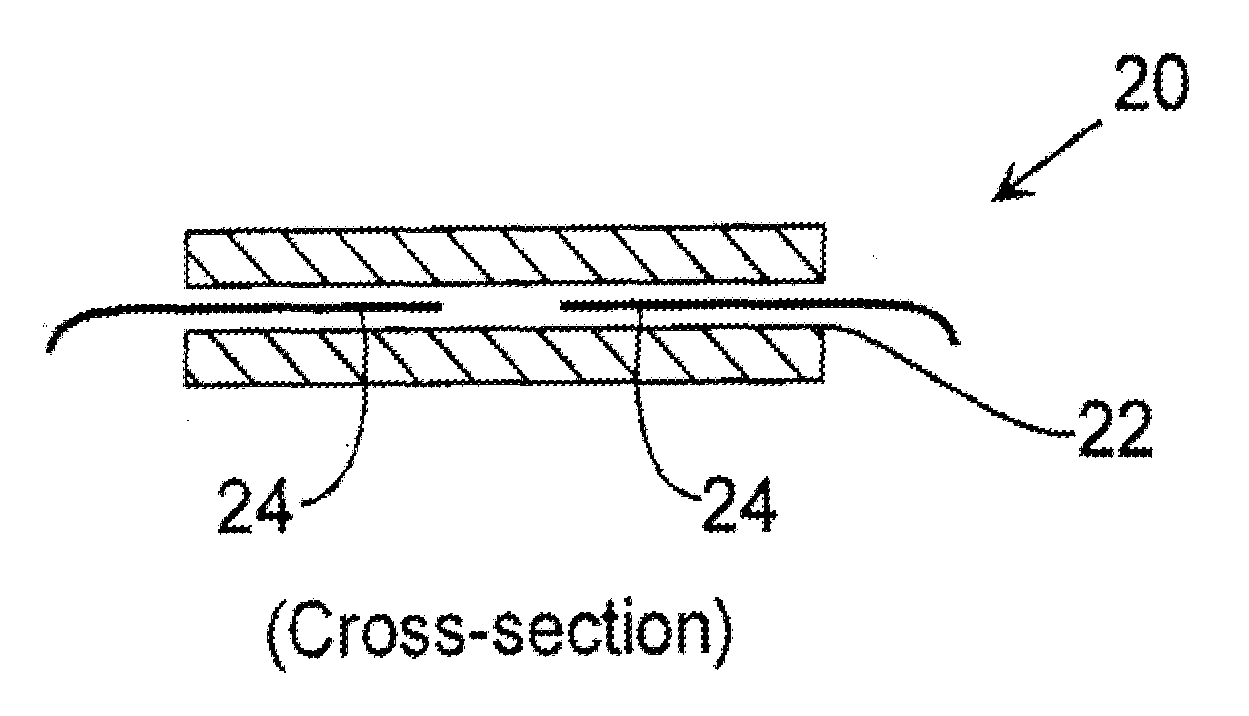
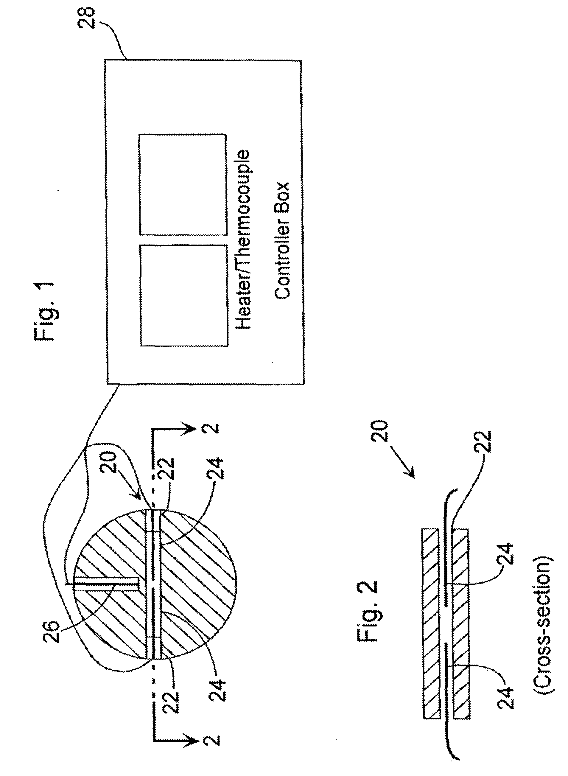
[0023]Reactor embodiment of the present invention can include heated electrode, deposition shield and / or other surfaces. By way of example only, FIGS. 1 and 2 depict plan and cross-sectional views of an upper electrode 20 for a reactor, and in particular of an etch reactor. The upper electrode has bores 22 provided therein which can receive heating elements 24. In this particular embodiment, two of the heating elements 24 are preferably cartridge heaters with an internal thermocouple. The third element 26 is a cartridge heater used as a thermocouple in order to sense the temperature. The cartridge heaters 24 and the cartridge heater 26 using a thermocouple are connected to a controller box 28 which uses the sensed temperature to maintain the level of heat generated by the cartridge heaters and thus the temperature of the upper electrode. In this preferred embodiment, the heaters are resistive type hea...


PUM

PropertyMeasurementUnit
temperatureaaaaaaaaaa

Abstract

A reactor for processing semiconductor wafers with electrodes and other surfaces that can be one of heated, textured and / or pre-coated in order to facilitate adherence of materials deposited thereon, and eliminate the disadvantages resulting from the spaulding, flaking and / or delaminating of such materials which can interfere with semiconductor wafer processing.

Description

CLAIM OF PRIORITY[0001]This application is a continuation of U.S. patent application Ser. No. 09 / 888,365, entitled “Reactor with Heated and Textured Electrodes and Surfaces,” by Stephen P. DeOrnellas, et al., filed Jun. 22, 2001 (Attorney Docket No. TEGL-01092US1), which is a continuation of U.S. patent application Ser. No. 09 / 453,842, entitled “Improved Reactor with Heated and Textured Electrodes and Surfaces,” by Stephen P. DeOrnellas, et al., filed Dec. 2, 1999, now abandoned. All of the above applications and patents are incorporated herein by reference.FIELD OF THE INVENTION[0002]The present invention is directed to reactors and in particular reactors for processing objects with films such as semiconductor wafers.BACKGROUND OF THE INVENTION[0003]During fabrication of semiconductor chips, wafers are processed in reactors which can accomplish various steps associated with the definition of the functionality of the semiconductor chip. Such reactors can, for example, perform deposi...

Claims


Application Information

Patent Timeline
Patent Type & Authority Applications(United States)
IPC IPC(8): H01L21/306C23C16/00C23C16/46C23C16/44H01J37/32H01L21/00H01L21/3065
CPCC23C16/4404H01J37/32009H01J37/32724H01L21/67069H01L21/67098
Inventor DEORNELLAS, STEPHEN P.JERDE, LESLIE G.OLSON, KURT A.
Owner OEM GROUP INC
Why Eureka
Try Eureka