Method of manufacturing light emitting element and method of manufacturing display apparatus having the same

a technology of light emitting elements and manufacturing methods, which is applied in the manufacture of electric discharge tubes/lamps, cold cathode manufacturing, and the manufacture of electromechanical systems, etc., can solve the problems of image display quality degradation of oled apparatuses, and achieve the effect of improving the illumination and uniformization of the display apparatus

Inactive Publication Date: 2008-04-17
LEE DONG WON +2
View PDF3 Cites 36 Cited by
  • Summary
  • Abstract
  • Description
  • Claims
  • Application Information

AI Technical Summary

Benefits of technology

[0016] The present invention provides a light emitting element capable of improving luminance and uniformity of the luminance.
[0022] Therefore, ejecting order of the light emitting material is controlled so that evaporation rate of volatile material in the light emitting material is not affected by adjacent light emitting patterns. Therefore, thicknesses of the light emitting patterns are uniformized so that luminance of the display apparatus is improved and uniformized.

Problems solved by technology

When the profiles of the light emitting patterns are different from one another, the OLED apparatus has non-uniform luminance so that an image display quality of the OLED apparatus is deteriorated.

Method used


Image

  • Method of manufacturing light emitting element and method of manufacturing display apparatus having the same
  • Method of manufacturing light emitting element and method of manufacturing display apparatus having the same
  • Method of manufacturing light emitting element and method of manufacturing display apparatus having the same

Examples


Embodiment Construction

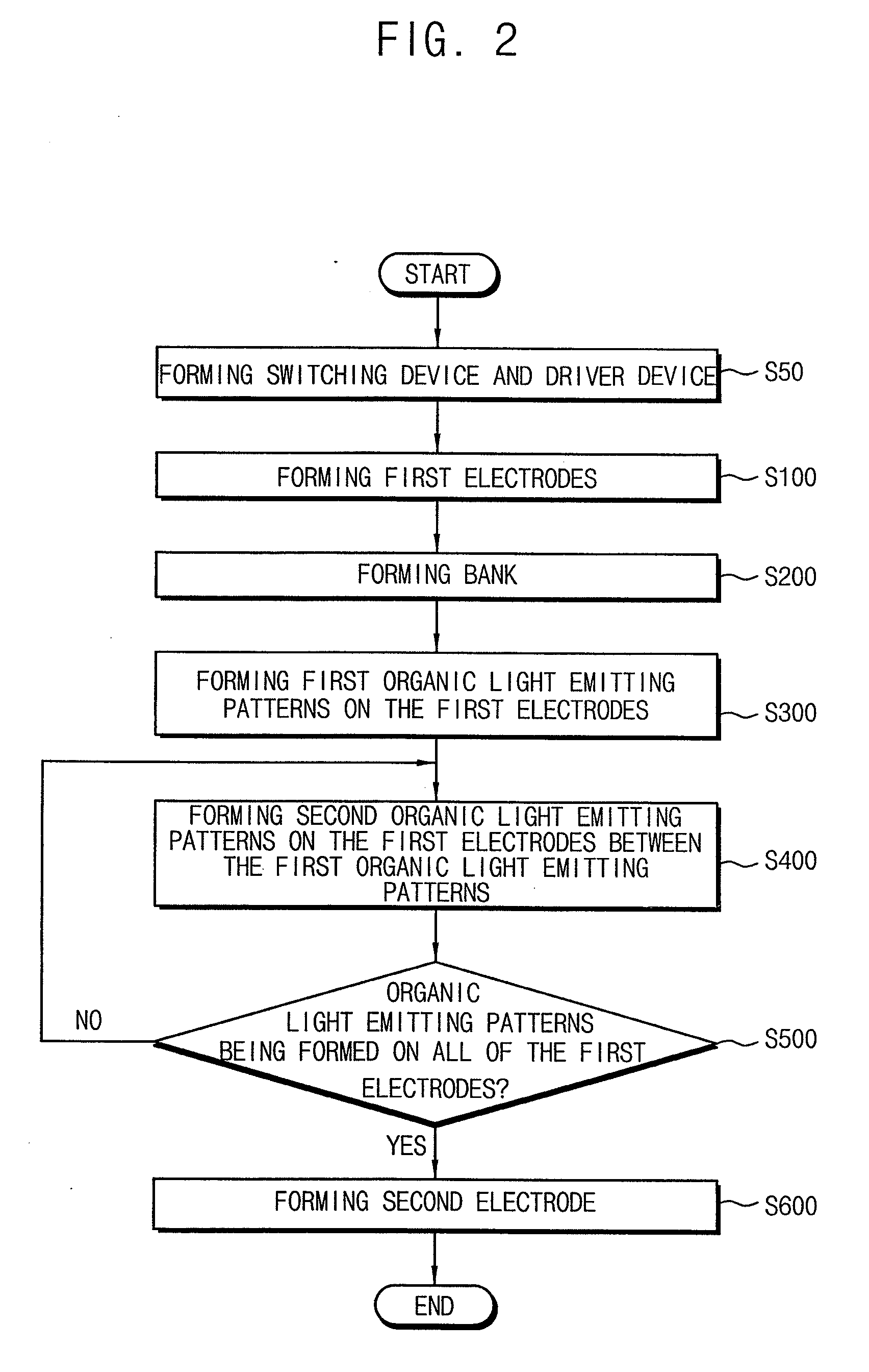
[0037] It should be understood that the exemplary embodiments of the present invention described below may be varied modified in many different ways without departing from the inventive principles disclosed herein, and the scope of the present invention is therefore not limited to these particular following embodiments. Rather, these embodiments are provided so that this disclosure will be through and complete, and will fully convey the concept of the invention to those skilled in the art by way of example and not of limitation.

[0038] Hereinafter, the present invention will be described in detail with reference to the accompanying drawings.

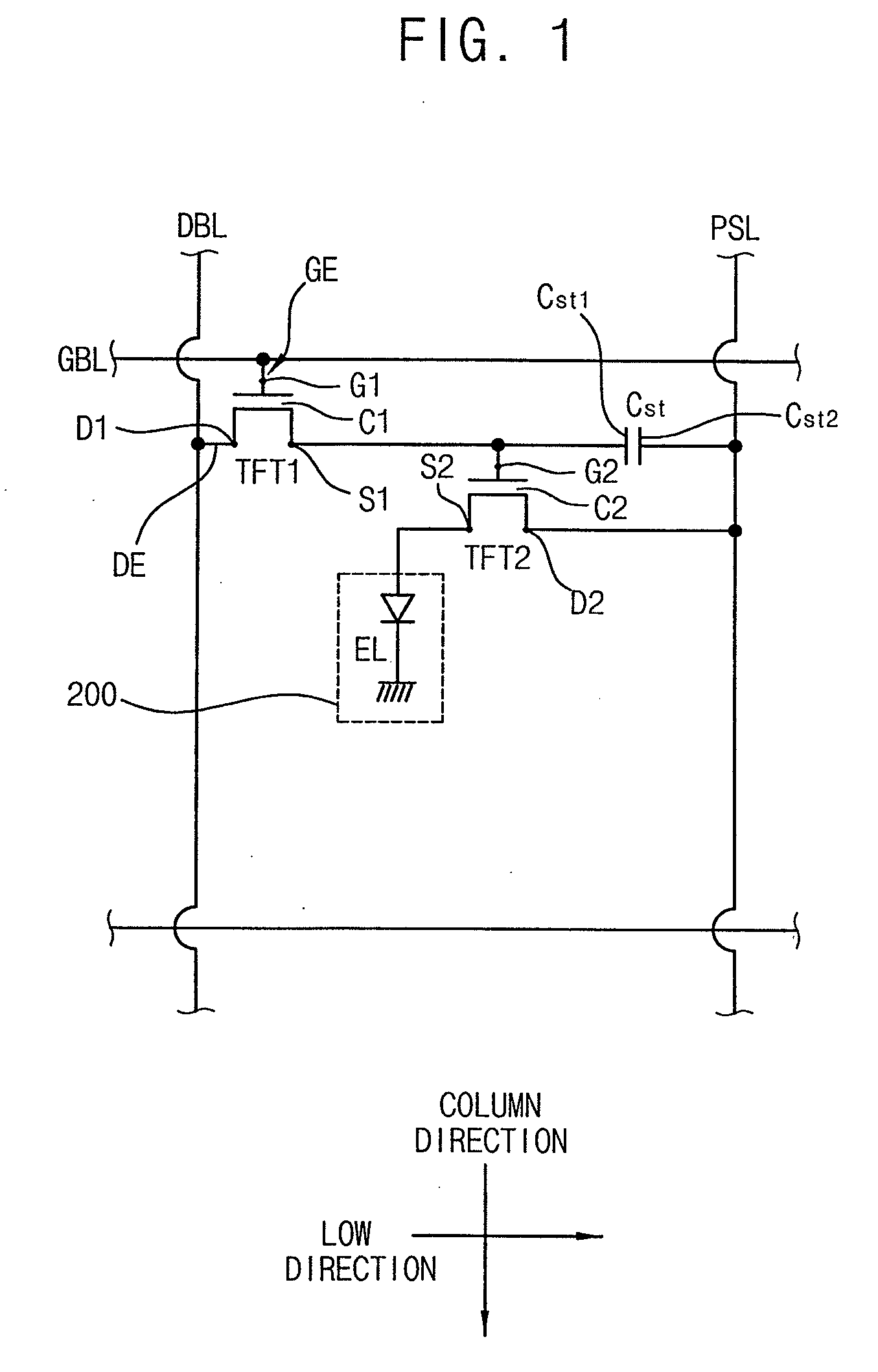
[0039]FIG. 1 is a circuit diagram showing a display apparatus in accordance with an exemplary embodiment of the present invention.

[0040] Referring to FIG. 1, the display apparatus includes a base substrate 100 of FIG. 3 and a display circuit. The display circuit has a switching device TFT1, a driver device TFT2, a light emitting element 200, a ...


PUM

PropertyMeasurementUnit
luminanceaaaaaaaaaa
uniformityaaaaaaaaaa
currentaaaaaaaaaa

Abstract

In a method of manufacturing a light emitting element, a plurality of first electrodes arranged in a matrix shape is formed on a pixel area of a base substrate. A bank is formed between the first electrodes. A light emitting material is ejected on a portion of the first electrodes spaced apart from one another to form a plurality of first light emitting patterns. The light emitting material is erected on a portion of the first electrodes between the first light emitting patterns to form a plurality of second light emitting patterns. A second electrode is formed on the first and second light emitting patterns. Therefore, a luminance of the light emitting element is improved and uniformized.

Description

CROSS-REFERENCE TO RELATED APPLICATIONS [0001] This application is a Divisional of U.S. application Ser. No. 11 / 017,532 filed on Dec. 20, 2004, which claims priority to Korean Application No. 2003-93741 filed on Dec. 19, 2003, the disclosure of which is hereby incorporated herein by reference in its entirety.BACKGROUND OF THE INVENTION [0002] 1. Field of the Invention [0003] The present invention relates to a method of manufacturing a light emitting element and a method of manufacturing a display apparatus having the light emitting element. More particularly, the present invention relates to a light emitting element capable of improving luminance and uniformity of the luminance and a method of manufacturing a display apparatus having the light emitting element. [0004] 2. Description of the Related Art [0005] A display apparatus, in general, converts data processed by an information processing device into an image. [0006] Display apparatuses includes a cathode ray tube (CRT) apparatu...

Claims


Application Information

Patent Timeline
Patent Type & Authority Applications(United States)
IPC IPC(8): H01J9/14H01J9/00H05B33/10H01J9/26H01L27/32H01L51/00H01L51/56
CPCH01L27/3211H01L27/3244H01L51/56H01L51/0005H01L27/3295H10K59/35H10K71/135H10K59/122H10K59/12H10K71/00H05B33/10
Inventor LEE, DONG-WONCHOI, JOON-HOOCHUNG, JIN-KOO
Owner LEE DONG WON
Why Eureka
Try Eureka