
Circuit board and electronic equipment

A circuit board and a sub-lead technology, which is applied to printed circuit components, conductive pattern layout details, printed circuits connected with non-printed electrical components, etc., can solve the problem of sparse lead arrangement, poor visual effect, and sub-lead area. Problems such as large visual differences, to achieve the effect of improving visual effects, improving user experience, and reducing visual differences

Pending Publication Date: 2022-01-07
LENOVO (BEIJING) CO LTD
View PDF3 Cites 0 Cited by
  • Summary
  • Abstract
  • Description
  • Claims
  • Application Information

AI Technical Summary

Problems solved by technology

[0002] At present, in the design of circuit boards of electronic equipment, there is often a problem that the visual difference of multiple sub-lead areas in the same lead area is relatively large due to the uneven arrangement density of the leads.
For example, on the touch screen of an electronic device, the circuit board corresponding to the touch screen is provided with a plurality of electrodes, and each motor needs to be connected with the drive controller, which will lead to The lead wires in the lead area are densely arranged, while the lead wires in the sub-lead area far away from the drive controller are sparsely arranged, so that the visual differences between different sub-lead areas in the lead area are relatively large, resulting in poor visual effects

Method used


Image

  • Circuit board and electronic equipment
  • Circuit board and electronic equipment
  • Circuit board and electronic equipment

Examples


Embodiment Construction

[0034] In order to enable those skilled in the art to better understand the technical solutions of the present application, the present application will be described in detail below in conjunction with the accompanying drawings and specific embodiments. Embodiments of the present application will be described in further detail below in conjunction with the accompanying drawings and specific embodiments, but this is not intended to limit the present application.

[0035] "First", "second" and similar words used in this application do not indicate any order, quantity or importance, but are only used to distinguish different parts. Words like "comprising" or "comprising" mean that the elements preceding the word cover the elements listed after the word, and do not exclude the possibility of also covering other elements. "Up", "Down", "Left", "Right" and so on are only used to indicate the relative positional relationship. When the absolute position of the described object changes...


PUM


Abstract

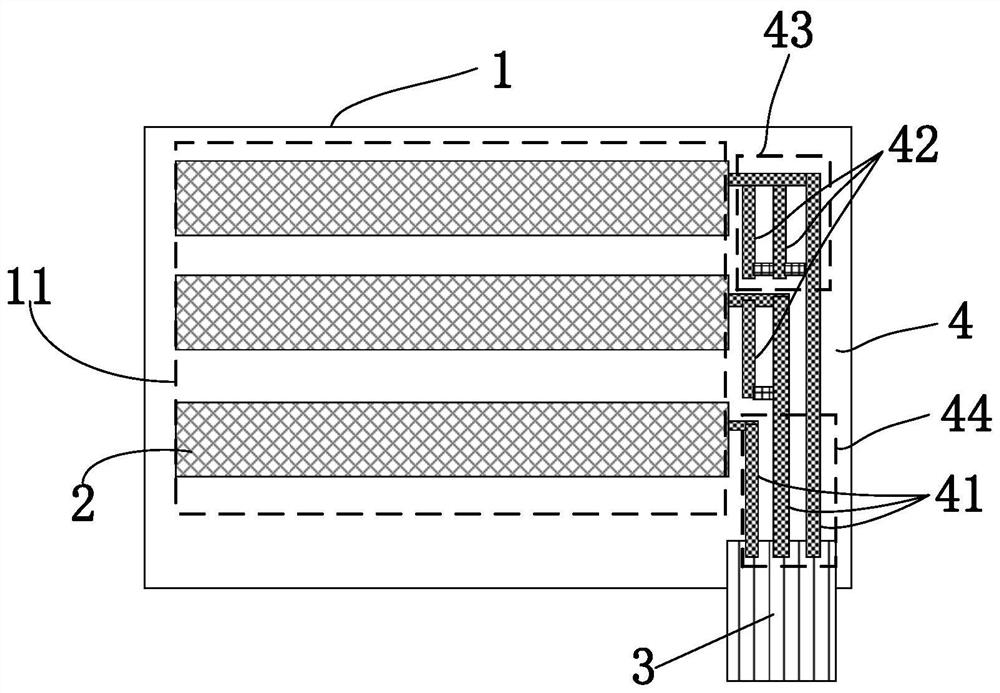
The embodiment of the invention provides a circuit board and electronic equipment. The circuit board comprises a substrate; a first board surface of the substrate comprises a first component and a second component which is a certain distance away from the first component; the first component is connected to the second component through a plurality of first leads; a first lead region is formed by a region through which the plurality of first leads pass; and second leads are arranged in at least one sub-lead areas sparsely arranged in the first lead region. With the above structure adopted, the visual difference of the different sub-lead areas can be reduced.

Description

technical field [0001] The present application relates to the field of electronic equipment, in particular to a circuit board and electronic equipment. Background technique [0002] At present, in the design of circuit boards of electronic equipment, there is often a problem of large visual differences between multiple sub-lead areas in the same lead area due to uneven arrangement density of the leads. For example, on the touch screen of an electronic device, the circuit board corresponding to the touch screen is provided with a plurality of electrodes, and each motor needs to be connected with the drive controller, which will lead to The lead wires in the lead area are densely arranged, while the lead wires in the sub-lead area far away from the drive controller are sparsely arranged, so that the visual differences between different sub-lead areas in the lead area are relatively large, resulting in poor visual effects . Contents of the invention [0003] Aiming at one o...

Claims


Application Information

Patent Timeline
Patent Type & Authority Applications(China)
IPC IPC(8): H05K1/02H05K1/18
CPCH05K1/0296H05K1/18
Inventor 张红娜朱泽力
Owner LENOVO (BEIJING) CO LTD
Learn More