A space-borne photoelectric conversion module and photoelectric detection device
A photoelectric conversion module and photoelectric detection technology, applied in the field of space detection, can solve problems such as high quality, achieve the effects of improving inheritance, shortening the development cycle, and improving the integration of arrays
- Summary
- Abstract
- Description
- Claims
- Application Information
AI Technical Summary
Problems solved by technology
Method used
Image
Examples
Embodiment 1
[0058] Figure 7 to 13 A star-loaded space photoelectric conversion module, including a photoelectric conversion device 205, an electronically reading circuit board 201 (hereinafter referred to as a PCB board) and a protective structure.
[0059] The photoelectric conversion device 205 is configured to convert the flash of the crystal 109 into an optoelectronics. In this embodiment, a relatively common photomultiplier (PMT) is employed. Since it is a glass device, the space-based beam device needs to experience extremely strong mechanics. The vibration environment is required to protect the buffer 204.
[0060] The protective structure also includes an internal bushing 207, a magnetic shield device 206, an outer bushing 203, and a buffer 204, and the inner bushing 207 and the outer bushing 203 are made of a magnesium aluminum alloy material, the magnetic shielding device. 206 is a slopolo-alloy sheet, and the buffer 204 can use silicone rubber of Sylgard 170, or other similar sili...
Embodiment 2
[0076] A starboard space photoelectric detection device comprising an array of photodetecting units and a thermally conductive bracket 3. like Figure 14 to 18 As shown, the photoelectric detector unit consists of a crystal module 1 and a photoelectric conversion module 2, and the structure of the photoelectric conversion module 2 is designed with embodiment one.
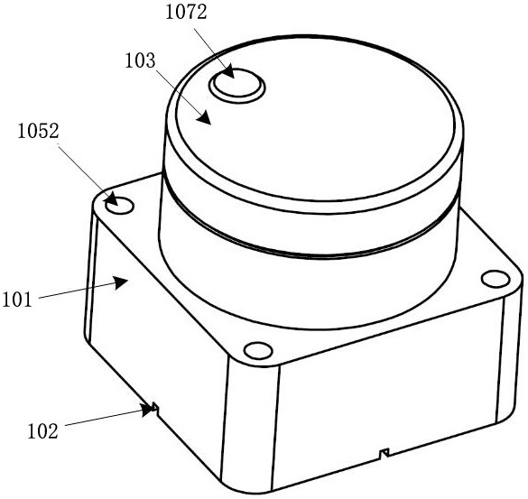
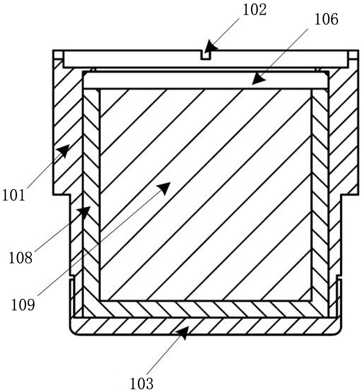
[0077] The structure of the crystal module 1, such as Figure 1 to 5 As shown, components include crystalline 109, crystal protection structure, temperature detection structure, performance scalar structure, and mounting interface.
PUM
| Property | Measurement | Unit |
|---|---|---|
| thickness | aaaaa | aaaaa |
| thickness | aaaaa | aaaaa |
| diameter | aaaaa | aaaaa |
Abstract
Description
Claims
Application Information
 - R&D
- Intellectual Property
- Life Sciences
- Materials
- Tech Scout
- Unparalleled Data Quality
- Higher Quality Content
- 60% Fewer Hallucinations
Browse by: Latest US Patents, China's latest patents, Technical Efficacy Thesaurus, Application Domain, Technology Topic, Popular Technical Reports.
© 2025 PatSnap. All rights reserved.Legal|Privacy policy|Modern Slavery Act Transparency Statement|Sitemap|About US| Contact US: help@patsnap.com


