A pcb board insulation lamination laying processing machine and method

A PCB board and processor technology, applied in multi-layer circuit manufacturing, electrical components, printed circuit manufacturing, etc., can solve problems such as high labor intensity, affecting the normal use of PCB boards, and disordered placement of core boards, so as to reduce efficiency, Extend the laying time and ensure the effect of neatness

Active Publication Date: 2020-07-17
深圳市兆兴博拓科技股份有限公司
View PDF9 Cites 0 Cited by
  • Summary
  • Abstract
  • Description
  • Claims
  • Application Information

AI Technical Summary

Problems solved by technology

[0003] However, the following problems exist in the laying process of the existing PCB insulation laminates: a. It is necessary to manually control the placement between the corresponding core board and the prepreg. The position is disordered, which affects the normal use of the PCB board. b. Manually controlling the placement of materials cannot ensure the orderliness of the laminated core boards. It is necessary to correct the laminated materials, which prolongs the laying time of the PCB insulation layer. Reduced laying efficiency
[0004] For the current technical problems in the production process of PCB boards, personnel in the relevant technical fields have conducted research and made adaptation improvements, such as the Chinese invention patent of a PCB board processing method with the patent number 200910109835X, which saves labor costs. The efficiency of burr repair is improved, but the difficulties in the laying process of the PCB insulation laminate mentioned above are not mentioned

Method used


Image

  • A pcb board insulation lamination laying processing machine and method
  • A pcb board insulation lamination laying processing machine and method
  • A pcb board insulation lamination laying processing machine and method

Examples


Embodiment Construction

[0033] The embodiments of the present invention will be described in detail below with reference to the accompanying drawings, but the present invention can be implemented in many different ways defined and covered by the claims.

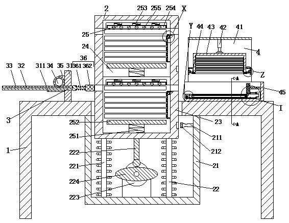
[0034] Such as Figure 1 to Figure 6 As shown, a PCB board insulation lamination laying processing machine includes an operation table 1, a lifting groove is provided in the middle of the operation table 1, an adjusting mechanism 2 is arranged in the lifting groove, and a pushing mechanism 3 is arranged on the left side of the operation table 1 , the right side of the console 1 is provided with a folding mechanism 4;

[0035] The adjustment mechanism 2 includes a lifting frame 21 installed on the lower end of the console 1, the lifting frame 21 is provided with an adjustment branch chain 22, and the adjustment branch chain 22 is equipped with a placement frame 23, and the inside of the placement frame 23 is uniformly provided with a placement cavity...


PUM


Abstract

The invention relates to a PCB insulation laminated layer laying processing machine and a PCB insulation laminated laying processing method. The PCB insulation laminated layer laying processing machine comprises an operation table, a lifting groove is formed in the middle of the operation table, and an adjusting mechanism is arranged in the lifting groove; a pushing mechanism is arranged at the left side of the operation table, and a laminating mechanism is arranged at the right side of the operation table. According to the invention, the following problems existing during the laying process of the existing PCB insulation lamination that a, the placement between a corresponding core plate and a prepreg needs to be controlled manually, the manual control operation labor intensity is high, and the core boards are easy to place disorderly during the placement process, so that the normal use of a PCB is influenced; b by manually controlling the placement of the materials, the uniformity ofthe corresponding core boards after lamination cannot be ensured, the laminated materials need to be corrected, the laying time of the insulating layers of the PCBs is prolonged, and the laying efficiency is reduced, can be solved.

Description

technical field [0001] The invention relates to the technical field of PCB board processing, in particular to a PCB board insulation lamination laying processing machine and method. Background technique [0002] The Chinese name of the PCB board is a printed circuit board, also known as a printed circuit board, which is an important electronic component, a support for electronic components, and a carrier for the electrical connection of electronic components. When the PCB board is made, the insulation laminate of the PCB board is composed of materials such as the base core board, the prepreg, and the insulation core board. The insulation laminate is mainly made by laying. [0003] However, the following problems exist in the laying process of the existing PCB insulation laminates: a. It is necessary to manually control the placement between the corresponding core board and the prepreg. The position is disordered, which affects the normal use of the PCB board. b. Manually co...

Claims


Application Information

Patent Timeline
Patent Type & Authority Patents(China)
IPC IPC(8): H05K3/46
CPCH05K3/4611H05K3/4638
Inventor 唐先华刘功利薄松姜锐
Owner 深圳市兆兴博拓科技股份有限公司
Why Eureka
Try Eureka