Display panel to be tested and testing method thereof, display panel and motherboard, display device
A display panel, a technology to be tested, applied in the field of display panels, motherboards, and display devices, which can solve problems such as the inability to click out solid-color images
- Summary
- Abstract
- Description
- Claims
- Application Information
AI Technical Summary
Problems solved by technology
Method used
Image
Examples
preparation example Construction
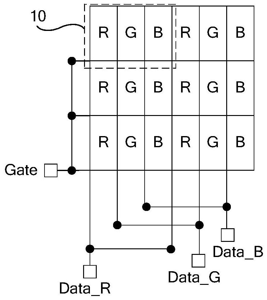
[0034] The preparation of display panels, such as TFT-LCD (Thin Film Transistor Liquid Crystal Display, thin film transistor-liquid crystal display) display panel preparation includes array (Array) substrate process, color filter (CF) substrate process and array substrate and color filter substrate. In the cell process, the panel function test is generally carried out during the cell process, and the defects of the substrate panel in the three processes of Array, CF, and Cell are used to remove the defective products before attaching the driver chip to improve the display. Yield of panel preparation. Usually, the display panel before the driver chip is pasted is referred to as the display panel to be inspected.
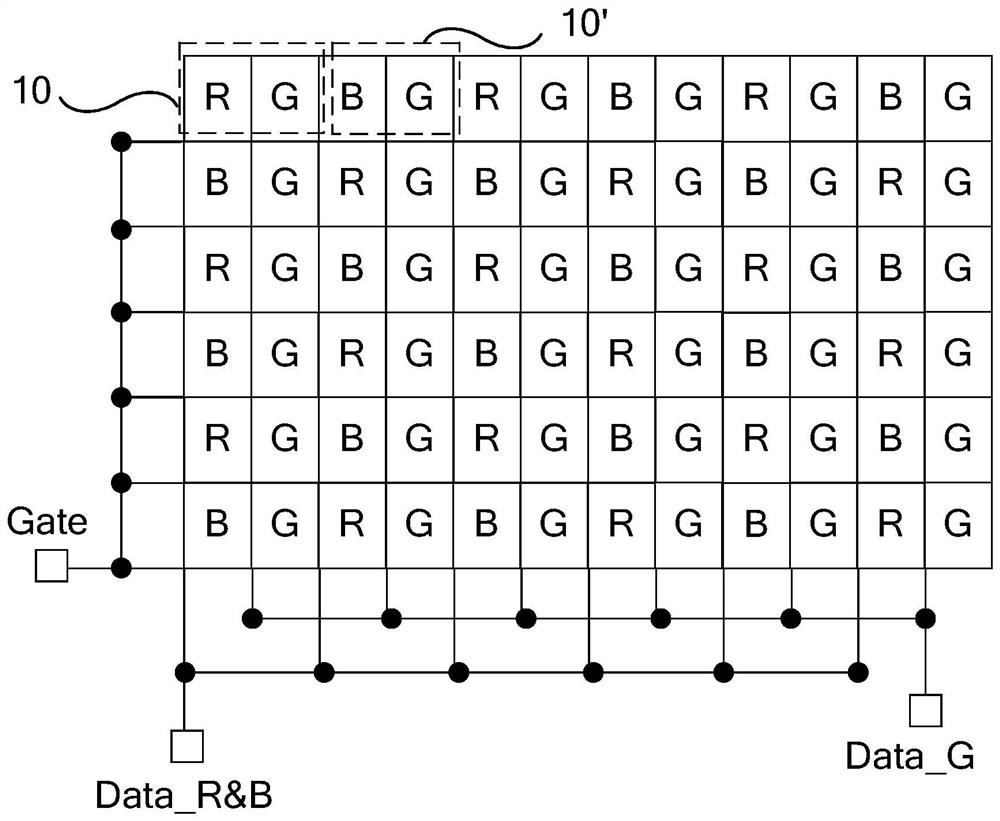
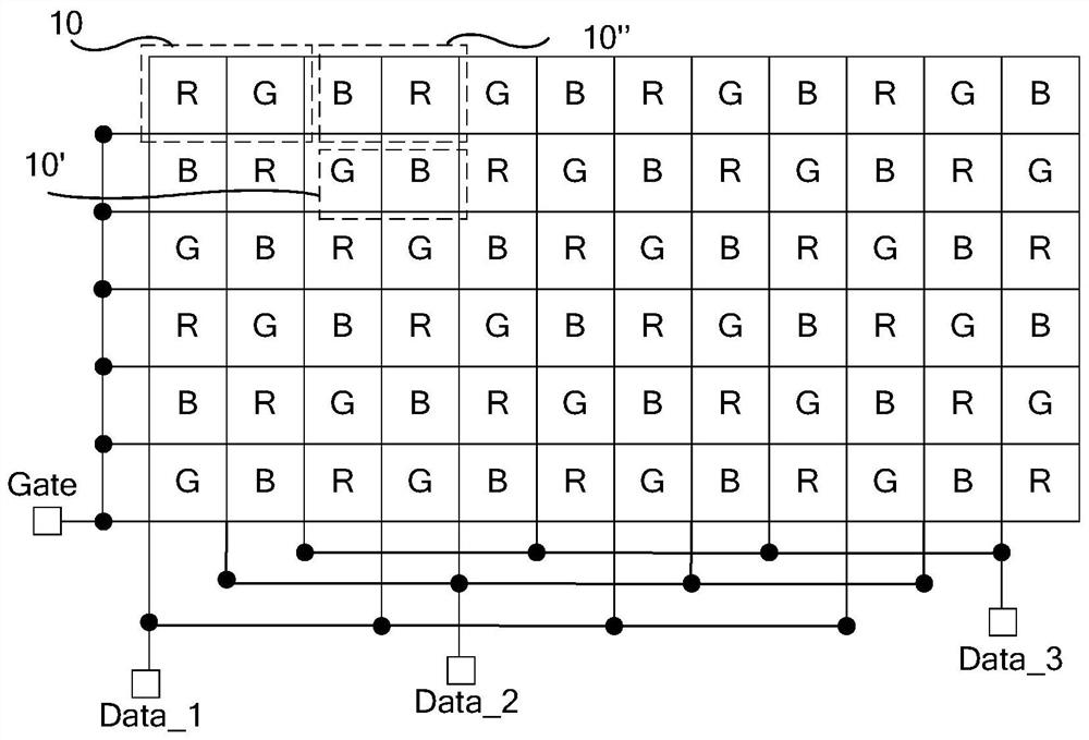
[0035] For a display panel using SPR technology, each pixel has sub-pixels of two colors, and the four sub-pixels corresponding to two adjacent pixels can cover the three colors provided by the display panel, for example figure 2 and image 3 As shown, pixel 10 has...
Embodiment 1
[0038] An embodiment of the present invention provides a display panel to be tested, such as Figure 4 and Figure 5 As shown, the display panel to be tested includes a sub-pixel array formed by multiple rows of sub-pixels and multiple columns of sub-pixels, each row of sub-pixels is driven by the same gate line, and each column of sub-pixels is driven by the same data line.
[0039] Wherein, all rows of sub-pixels with the same color distribution in multiple rows of sub-pixels form a row pixel group, and multiple rows of sub-pixels constitute at least two row pixel groups; at least two of the gate lines used to drive each row pixel group Electrically connected via connecting wires.
[0040] All the column sub-pixels with the same color distribution in the multiple columns of sub-pixels form a column pixel group, and the multiple columns of sub-pixels form at least two column pixel groups; at least two of the data lines used to drive each column pixel group are electrically c...
Embodiment 2
[0056] This embodiment provides a detection method of the display panel to be detected as described in Embodiment 1, the detection method can drive all sub-pixels of a color in the display panel to be detected to display, including the following steps:
[0057] Sequentially input the row driving signal to the gate line corresponding to each row pixel group, and input the data signal to the data line corresponding to the column pixel group to which the sub-pixel of the above color in the row pixel group belongs, so as to sequentially light up the above-mentioned colors in each row pixel group of sub-pixels.
[0058] It should be noted that the gate lines corresponding to a row of pixel groups refer to all the gate lines used to drive the row of pixel groups. Wherein, the row driving signals are respectively input to the gate lines of each row of pixel groups, the gate lines of each row of pixel groups receive the row driving signals at the same time, and while the row driving s...
PUM
 Abstract
Description
Claims
Application Information
 - Generate Ideas
- Intellectual Property
- Life Sciences
- Materials
- Tech Scout
- Unparalleled Data Quality
- Higher Quality Content
- 60% Fewer Hallucinations
Browse by: Latest US Patents, China's latest patents, Technical Efficacy Thesaurus, Application Domain, Technology Topic, Popular Technical Reports.
© 2025 PatSnap. All rights reserved.Legal|Privacy policy|Modern Slavery Act Transparency Statement|Sitemap|About US| Contact US: help@patsnap.com


