Manufacturing method of multilayer circuit board

A technology of a multilayer circuit board and a manufacturing method, which is applied in the field of communication and can solve the problems of double-sided circuit diagram damage, circuit diagram deformation, unusability of the multilayer circuit board, etc.

Active Publication Date: 2019-11-08
NEW FOUNDER HLDG DEV LLC +1
View PDF5 Cites 0 Cited by
  • Summary
  • Abstract
  • Description
  • Claims
  • Application Information

AI Technical Summary

Problems solved by technology

[0005] The embodiment of the present invention provides a method for manufacturing a multilayer circuit board, to solve the problem that when both board surfaces of the polytetrafluoroethylene double-sided board are subjected to tangential flow viscous friction during the manufacturing process of the multilayer circuit board, under high temperature conditions The pull of the force caused the deformation of the circuit diagrams on both boards of the double-sided board. The circuit diagrams on the two boards were relatively deformed, resulting in serious damage to the circuit diagrams of the double-sided board, which led to the unusable problem of the multi-layer circuit board.

Method used


Image

  • Manufacturing method of multilayer circuit board
  • Manufacturing method of multilayer circuit board

Examples


Embodiment Construction

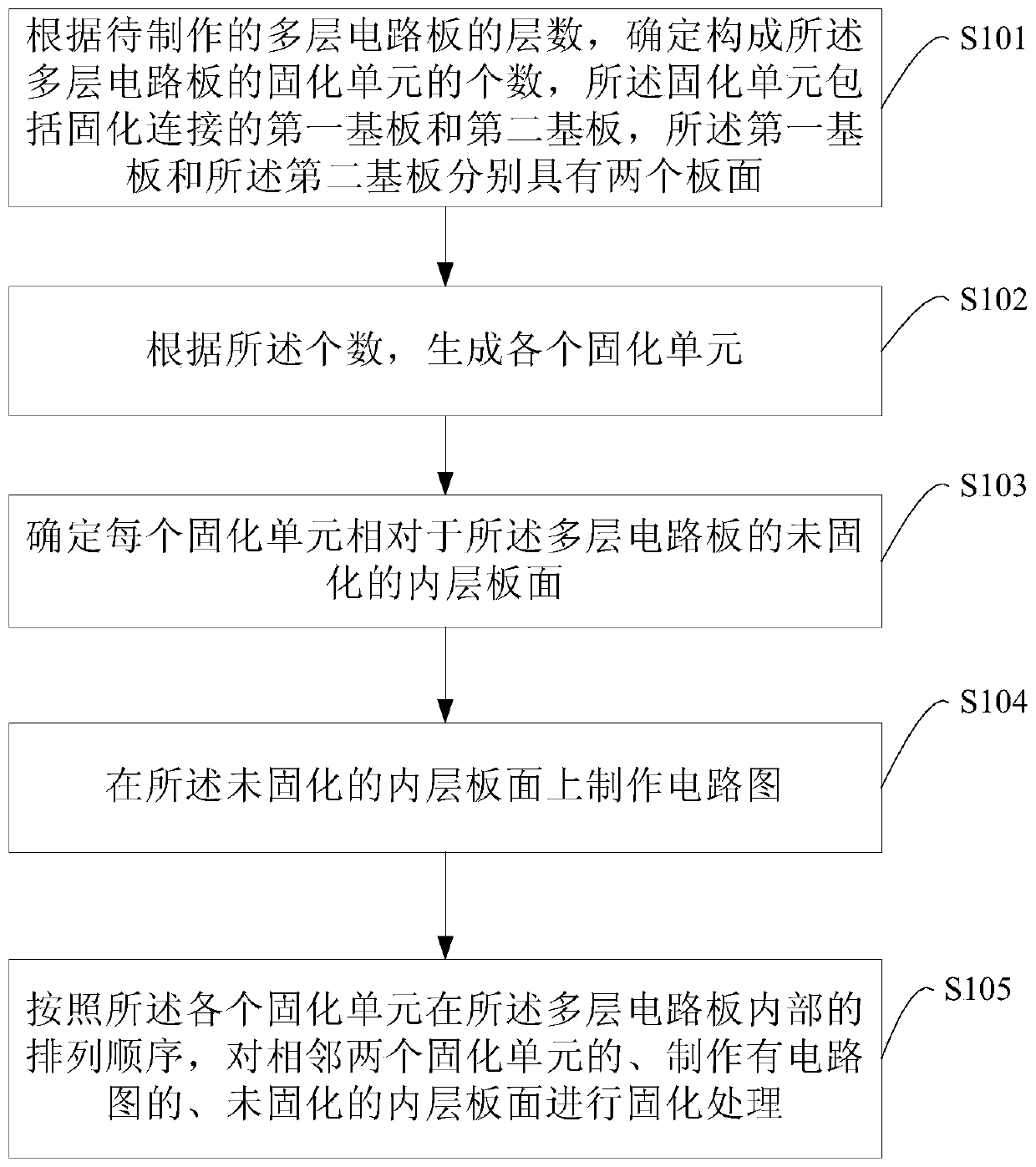
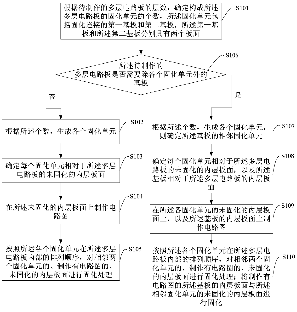
[0015] In practical applications, when receiving the customer's demand for making a multi-layer circuit board, according to the customer's needs, the technicians will analyze the stack structure of the multi-layer circuit board to be produced, including substrate materials, prepreg materials, buried drilling, blind drilling and other information, so as to determine the number of layers of the multilayer circuit board to be made, and pre-design the design engineering design circuit diagram, MI instruction (Manufacturing Instruction, production instruction) and CAM (computer Aided Manufacturing, computer-aided Production) data, you can control the production process of multi-layer circuit boards through pre-set MI instructions and CAM data.

[0016] figure 1 It is a flow chart of the manufacturing method of the multilayer circuit board provided by Embodiment 1 of the present invention. The embodiment of the present invention aims at the fact that in the manufacturing process of...


PUM


Abstract

The invention provides a manufacturing method of a multi-layer circuit board. The method comprises steps that according to the layer number of a to-be-manufactured multi-layer circuit board, the number of solidification units for forming the multi-layer circuit board is determined, the solidification units comprise first substrates and second substrates which are in solidification connection, andthe first substrates and the second substrates respectively have two board surfaces; according to the number, the various solidification units are generated; a non-solidification inner board surface of each solidification unit opposite to the multi-layer circuit board is determined; a circuit diagram is made on the non-solidification inner board surface; according to the ordering sequence of the solidification units in the multi-layer circuit board, and the non-solidification inner board surface which is adjacent to two solidification units and is provided with the circuit diagram is solidified. The method is advantaged in that for the manufactured multi-layer circuit board, severe damage to the circuit diagrams belonging to two board surfaces of one substrate because of severe relative deformation caused by tangential viscous friction can be avoided, and the manufactured multi-layer circuit board can be utilized.

Description

technical field [0001] Embodiments of the present invention relate to the field of communication technologies, and in particular, to a method for manufacturing a multilayer circuit board. Background technique [0002] A multi-layer circuit board is made by pressing multiple double-sided boards (that is, core). For example, a four-layer circuit board is made by pressing two double-sided boards. Prepreg, under high temperature and high pressure conditions, the resin glue in the prepreg flows from the center of the panel to the surroundings, and fully fills the gap between the lines and the copper-free area on the adjacent board. In a pressing process, the board surface cured with the prepreg is called the inner board surface, and the board surface not cured with the prepreg is called the outer board surface. [0003] During the pressing process, when the resin glue flows from the center of the double-sided panel to the surroundings, a tangential flow viscous friction force is...

Claims


Application Information

Patent Timeline
Patent Type & Authority Patents(China)
IPC IPC(8): H05K3/46
CPCH05K3/4611H05K2203/061
Inventor 陈显任柳小华李晓
Owner NEW FOUNDER HLDG DEV LLC
Why Eureka
Try Eureka