A vdmos device with seb resistance

A device and capability technology, which is applied in the field of semiconductor devices, can solve the problems of limited function and the concentration of the Pbody region should not be too large, and achieve the effect of preventing opening and improving the anti-SEB ability

Active Publication Date: 2020-07-31
UNIV OF ELECTRONICS SCI & TECH OF CHINA
View PDF3 Cites 0 Cited by
  • Summary
  • Abstract
  • Description
  • Claims
  • Application Information

AI Technical Summary

Problems solved by technology

Considering the impact on the device threshold, the concentration of the Pbody region should not be too large, so the method of reducing the resistance under the N+ source region of the VDMOS device by increasing the concentration of the Pbody has limited effect

Method used


Image

  • A vdmos device with seb resistance
  • A vdmos device with seb resistance
  • A vdmos device with seb resistance

Examples


Embodiment 1

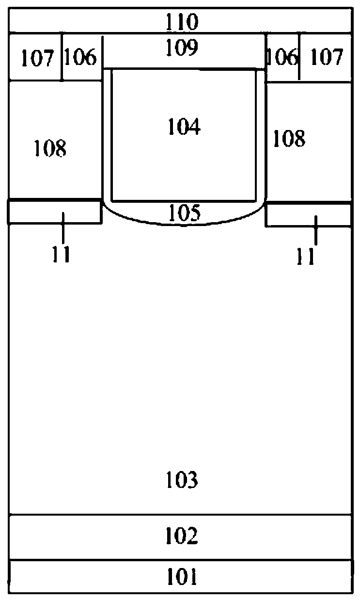
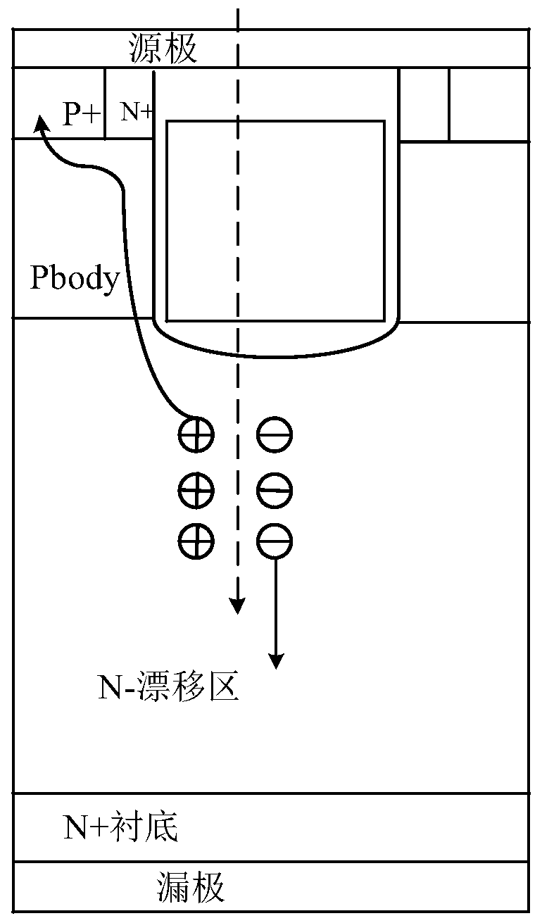
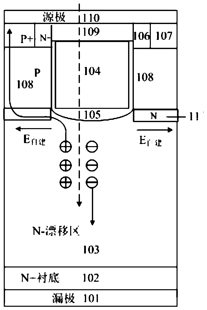
[0019] Such as figure 1 As shown, a VDMOS device with anti-SEB capability is sequentially stacked with a metallized drain 101, a first conductivity type semiconductor substrate 102, a first conductivity type semiconductor epitaxial layer 103, and a metallized source 110 from bottom to top; The left and right sides of the upper surface of the first conductivity type semiconductor epitaxial layer 103 respectively have second conductivity type semiconductor body regions 108; the inner upper surface of each second conductivity type semiconductor body region 108 has a first conductivity type semiconductor source region 106 and a second conductivity type semiconductor body region 106. The second conductivity type semiconductor body contact region 107; the first conductivity type semiconductor source region 106 and the second conductivity type semiconductor body contact region 107 are connected to the metallized source 110; the second conductivity type semiconductor body region 108 on...

Embodiment 2

[0025] Such as Figure 4 As shown, the structure of this example is based on Embodiment 1. The carrier guide region 11 of the first conductivity type semiconductor under the second conductivity type semiconductor body region 108 includes n different doping concentrations in the lateral direction. The sub-regions 111 , 112 . . . 11n, n is greater than or equal to 3, and the doping concentration of the sub-regions satisfies: as the distance from the polysilicon gate electrode 104 gradually increases, the doping concentration of the sub-regions gradually decreases.


PUM


Abstract

The invention provides a VDMOS device with anti-SEB capability, which sequentially stacks a metallized drain, a first conductivity type semiconductor substrate, a first conductivity type semiconductor epitaxial layer, and a metallization source from bottom to top; it also includes a second conductivity type Type semiconductor body region, first conductivity type semiconductor source region, second conductivity type semiconductor body contact region, there is a gate structure between the second conductivity type semiconductor body regions on both sides; the present invention adopts the second conductivity type semiconductor body region The bottom of the bottom introduces a carrier guide region, and the impurity distribution in the guide region can generate a self-built electric field, which can guide carriers to avoid flowing through the semiconductor body region of the second conductivity type directly below the semiconductor source region of the first conductivity type part, thereby preventing the opening of the parasitic triode and improving the anti-SEB capability of VDMOS during single event radiation.

Description

technical field [0001] The invention relates to the technical field of semiconductor devices, in particular to a VDMOS device with anti-SEB capability. Background technique [0002] With the rapid development of power electronics technology to high-frequency and high-power applications, VDMOS has become one of the irreplaceable important devices in the field of power electronics, and power electronic circuits using VDMOS are increasing. The device with this structure is usually formed by secondary diffusion or ion implantation technology. It is a multi-cell device, easy to integrate, high power density, multi-carrier conduction, and good frequency characteristics. At present, VDMOS is one of the mainstream devices of power MOS. As a power switch, VDMOS has the advantages of high withstand voltage, fast switching speed, low on-resistance, low drive power, good thermal stability, low noise and simple manufacturing process, and is widely used in switching power supplies, AC dr...

Claims


Application Information

Patent Timeline
Patent Type & Authority Patents(China)
IPC IPC(8): H01L29/78H01L29/06
Inventor 任敏林育赐苏志恒何文静李泽宏张波
Owner UNIV OF ELECTRONICS SCI & TECH OF CHINA
Why Eureka
Try Eureka