A Nano-Silicon Oxide Insulator for Vfto Suppression
A nano-silicon oxide, insulator technology, applied in insulators, electrical components, circuits, etc., can solve the problems of surface charge accumulation on insulators and unstable operation of GIS equipment, and achieve the effect of reducing charge accumulation and maintaining reliability.
- Summary
- Abstract
- Description
- Claims
- Application Information
AI Technical Summary
Problems solved by technology
Method used
Image
Examples
Embodiment 1
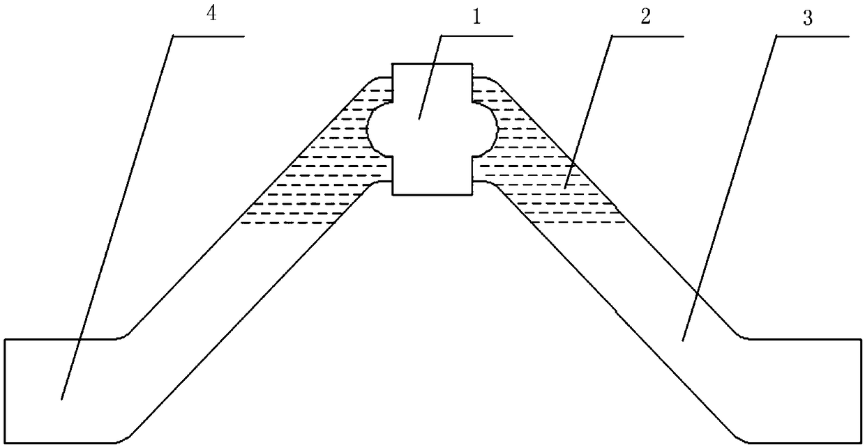
[0024] figure 1 A schematic structural diagram of a nano-silicon oxide insulator for suppressing VFTO provided by the embodiment of the present application. see figure 1 , the insulator includes: a central insert 1 , an insulating area 2 , a nano-silicon oxide creepage area 3 and a fixing flange 4 . Wherein, the central insert 1 is arranged on the top of a hollow cone, and the cone is divided into two parts, wherein one end close to the central insert 1 is an insulating region 2, and the rest is a nano-silicon oxide creepage region 3, The bottom of the nano-silicon oxide creepage region 3 is connected to the fixing flange 4 . That is to say, the longitudinal section of the insulator is a "V"-shaped structure.
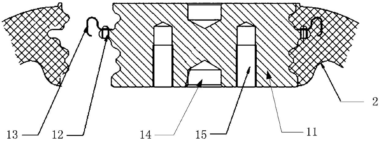
[0025] Optionally, the insulating region 2 provided in the embodiment of the present application is an epoxy resin-based alumina margin region, wherein the addition amount of alumina can be any value between 5% and 10%, for example, 8%. It should be noted that the c...
Embodiment 2
[0033] The various parts of the insulator provided in Example 1 of the present application, including the central insert 1, the insulating area 2, the nano-silicon oxide creepage area 3 and the fixing flange 4, are integrated connection structures, rather than being connected by bolts, screws, etc. of. This embodiment mainly describes the preparation method of the insulator.
[0034] The integrated insulator provided in the embodiment of the present application is prepared by vacuum casting. During the operation of GIS, under the action of VFTO, charges will be introduced on the surface of the insulator. Compared with the bolt connection, the integrated connection structure is beneficial to reduce the resistance of the insulator itself, and facilitate the dissipation of the charges accumulated on the surface of the insulator.
[0035] Specifically, the preparation method of the integrated insulator provided in the embodiment of the present application is as follows:
[0036...
Embodiment 3
[0040] In this embodiment, insulators with nano-silicon oxide additions of 0%, 5% and 10% in the nano-silicon oxide creepage region 3 were respectively used to carry out VFTO wave application experiments to detect the effect of the insulator on the dissipation of surface charges, as follows shown.
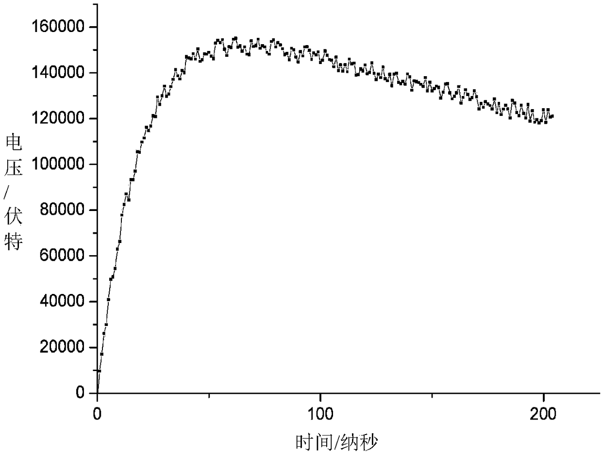
[0041] image 3 The VFTO waveform diagram applied at the center insert 1 provided in the embodiment of the present application. Apply the VFTO wave at the central insert 1 of each of the above insulators, and collect the surface potential data from the high-voltage electrode to the fixed flange 4 on the surface of each insulator, and obtain the following: Figure 4 The potential diagram of the high voltage electrode to the fixing flange 4 of the insulator is shown.
[0042] From Figure 4 It can be seen that the surface potential of the insulator with the addition of 0% nano-silicon oxide in the nano-silicon oxide creepage region 3 is the highest, followed by the insulator with th...
PUM
 Abstract
Description
Claims
Application Information
 - R&D
- Intellectual Property
- Life Sciences
- Materials
- Tech Scout
- Unparalleled Data Quality
- Higher Quality Content
- 60% Fewer Hallucinations
Browse by: Latest US Patents, China's latest patents, Technical Efficacy Thesaurus, Application Domain, Technology Topic, Popular Technical Reports.
© 2025 PatSnap. All rights reserved.Legal|Privacy policy|Modern Slavery Act Transparency Statement|Sitemap|About US| Contact US: help@patsnap.com


