An inclined silicon pinpoint and a manufacturing method thereof

A manufacturing method and a tilting technology, which are applied in the field of micro-nano device preparation, can solve problems such as the inability to meet the needs of near-field optical real-time observation, and achieve the effects of being suitable for large-scale production, simple manufacturing methods, and cheap and readily available raw materials

Active Publication Date: 2017-05-03
SUZHOU INST OF NANO TECH & NANO BIONICS CHINESE ACEDEMY OF SCI
View PDF8 Cites 4 Cited by
  • Summary
  • Abstract
  • Description
  • Claims
  • Application Information

AI Technical Summary

Problems solved by technology

The silicon needle tips prepared by the above existing processes are basically vertical needle tips, which cannot meet the needs of near-field optics for real-time observation

Method used


Image

  • An inclined silicon pinpoint and a manufacturing method thereof
  • An inclined silicon pinpoint and a manufacturing method thereof
  • An inclined silicon pinpoint and a manufacturing method thereof

Examples


Embodiment Construction

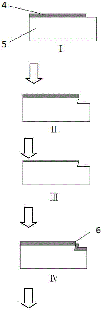
[0027] As mentioned above, in view of the shortcomings in the prior art, the inventor of the present case, after long-term research and extensive practice, specially proposed the technical solution of the present invention, and obtained unexpectedly good technical effects. The technical solutions of the present invention will be explained in more detail in conjunction with the embodiments and the drawings as follows.

[0028] See Figure 1-2 , Which shows a typical implementation case of the present invention.

[0029] Further, please refer to figure 1 , This embodiment relates to an inclined silicon tip, which is a triangular pyramid and has a first inclined surface, a second inclined surface, a third inclined surface and a bottom surface, and the first inclined surface, the second inclined surface and The angles between at least two of the third inclined surfaces and the bottom surface are not equal.

[0030] Wherein, the angle between the first inclined surface and the bottom su...


PUM

PropertyMeasurementUnit
heightaaaaaaaaaa
diameteraaaaaaaaaa

Abstract

The invention discloses an inclined silicon pinpoint and a manufacturing method thereof. The pinpoint is a triangular pyramid and has a first inclined surface, a second inclined surface, a third inclined surface and a bottom surface, and the angles between at least two of the first inclined surface, the second inclined surface and the third inclined surface and the bottom surface are not equal. The manufacturing method comprises the following steps: forming a first and a second inclined surface of the inclined silicon pinpoint by applying an isotropic etching process on a silicon wafer; then providing protective layers on the first and second inclined surfaces; and afterwards, processing the silicon wafer with an etching process to form a third inclined surface to obtain a target product. The invention provides the inclined silicon pinpoint which is different from traditional silicon pinpoints and can satisfy demands of near-field optics for real time observation; the manufacturing method is simple; the raw materials are cheap and easily available; the inclined silicon pinpoint is suitable for large scale production; and a new path is provided for popularization and application of pinpoints.

Description

Technical field [0001] The invention mainly relates to a silicon needle tip, in particular to an inclined silicon needle tip and a manufacturing method thereof, and belongs to the field of micro-nano device preparation. Background technique [0002] In recent years, silicon-based nanotips have been widely used in atomic force microscope probes, vacuum microelectronic devices, field emission devices, high-density data storage devices, nanoscale pattern processing, and micromechanical tunnel sensors. The key components, the performance of these devices depends on the radius of curvature and needle shape of the nano-tip. Taking the atomic force microscope as an example, the larger the aspect ratio of the silicon tip and the smaller the radius of curvature, the higher the resolution of the atomic force microscope. Therefore, it is of great significance to study the fabrication of silicon-based nanometer tips. Currently, there are three common methods for preparing silicon-based nano...

Claims


Application Information

Patent Timeline
Patent Type & Authority Applications(China)
IPC IPC(8): G01Q70/16
CPCG01Q70/16
Inventor 李加东苗斌吴东岷
Owner SUZHOU INST OF NANO TECH & NANO BIONICS CHINESE ACEDEMY OF SCI
Why Eureka
Try Eureka