Broadband electromagnetic absorber with adjustable absorption rate based on graphene film
A graphene film, wave absorber technology, applied in electrical components, antennas and other directions, can solve the problems of poor practicability and high cost, reduce the impact of performance, reduce manufacturing difficulty and cost, and change the effect of input impedance
- Summary
- Abstract
- Description
- Claims
- Application Information
AI Technical Summary
Problems solved by technology
Method used
Image
Examples
Embodiment 1
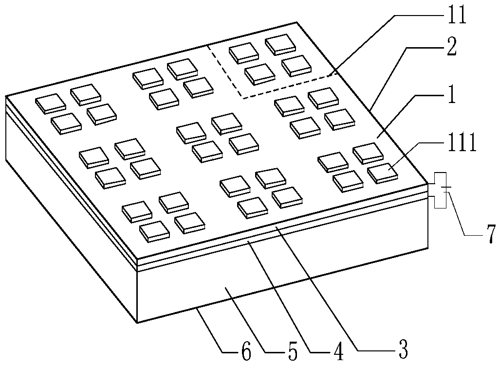
[0018] refer to figure 1 , a broadband electromagnetic absorber with adjustable absorption rate based on graphene film, including a conductive layer and a dielectric layer stacked up and down: the conductive layer includes a metal patch 1 and a graphene film attached to its lower surface 2. The metal patch 1 is etched with a plurality of cross-shaped slits in different forms to form M×N patch units 11, where M>2, N>2, and each patch unit 11 consists of m×n pieces Composed of patches 111, where m>2, n>2; the dielectric layer includes a first dielectric board 3, a second dielectric board 4 and a third dielectric board 5 stacked from top to bottom, wherein the first dielectric board 3 adopts Insulating material, the second dielectric board 4 is made of semiconductor material; the bottom surface of the third dielectric board 5 is printed with a bottom board 6 . A DC power supply 7 is connected between the graphene film 2 and the second dielectric plate 4 for adjusting the surface...
Embodiment 2
[0036] Embodiment 2 has the same structure as Embodiment 1, only the material of the third dielectric plate 5 and the relative permittivity ε r3 Made an adjustment: the third dielectric plate 5 selects the relative permittivity ε r3 4 polymethacrylate (PMMA) dielectric board.
Embodiment 3
[0038] Embodiment 3 has the same structure as Embodiment 1, only the material of the third dielectric plate 5 and the relative permittivity ε r3 Made an adjustment: the third dielectric plate 5 selects the relative permittivity ε r3 1.05 foam medium board.
[0039] Below in conjunction with simulation experiment, technical effect of the present invention is described further:
[0040] 1. Simulation conditions and content
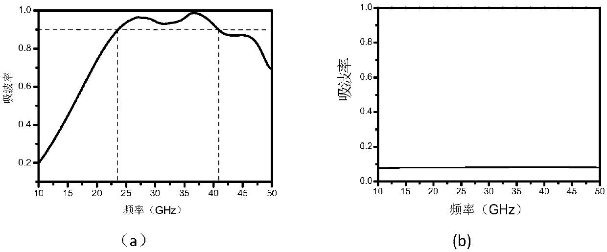
[0041] Utilize the commercial simulation software HFSS_13.0 to carry out the simulation calculation of the absorption rate curve of the wave absorber under different DC power supply voltages in the above-mentioned embodiment 1, the result is as follows image 3 shown.
[0042] 2. Simulation results
[0043] refer to image 3 , the abscissa in the figure is the frequency, the unit is GHz, the range is 10GHz-50GHz, and the ordinate indicates the normalized absorbed electromagnetic wave energy, the range is 0.1-1. from image 3 (a) It can be seen that th...
PUM
 Abstract
Description
Claims
Application Information
 - R&D
- Intellectual Property
- Life Sciences
- Materials
- Tech Scout
- Unparalleled Data Quality
- Higher Quality Content
- 60% Fewer Hallucinations
Browse by: Latest US Patents, China's latest patents, Technical Efficacy Thesaurus, Application Domain, Technology Topic, Popular Technical Reports.
© 2025 PatSnap. All rights reserved.Legal|Privacy policy|Modern Slavery Act Transparency Statement|Sitemap|About US| Contact US: help@patsnap.com


