Far-infrared wide-band cyclical absorber structure
A wide-band, far-infrared technology, applied in electrical components, antennas, etc., can solve the problems of narrow absorption frequency band and single frequency band
- Summary
- Abstract
- Description
- Claims
- Application Information
AI Technical Summary
Problems solved by technology
Method used
Image
Examples
Embodiment Construction
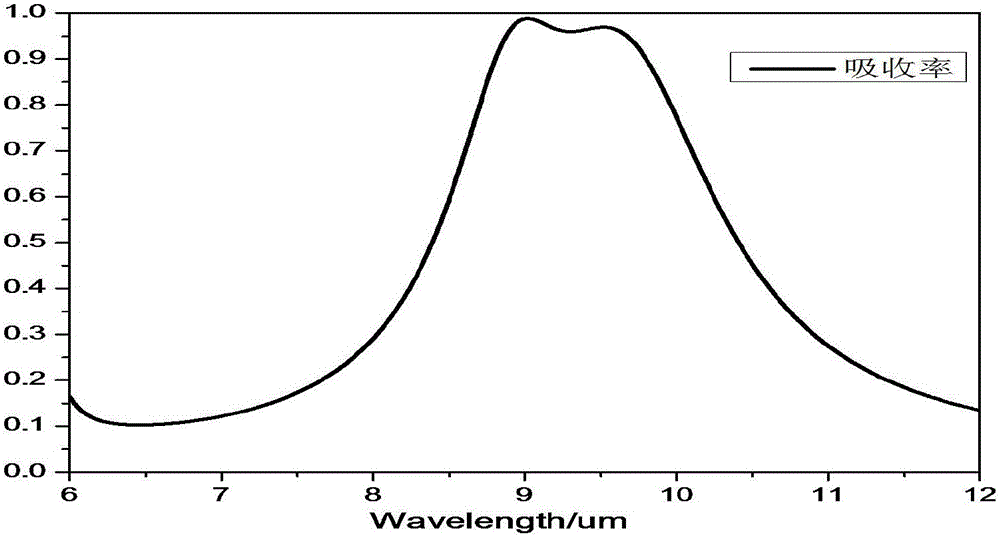
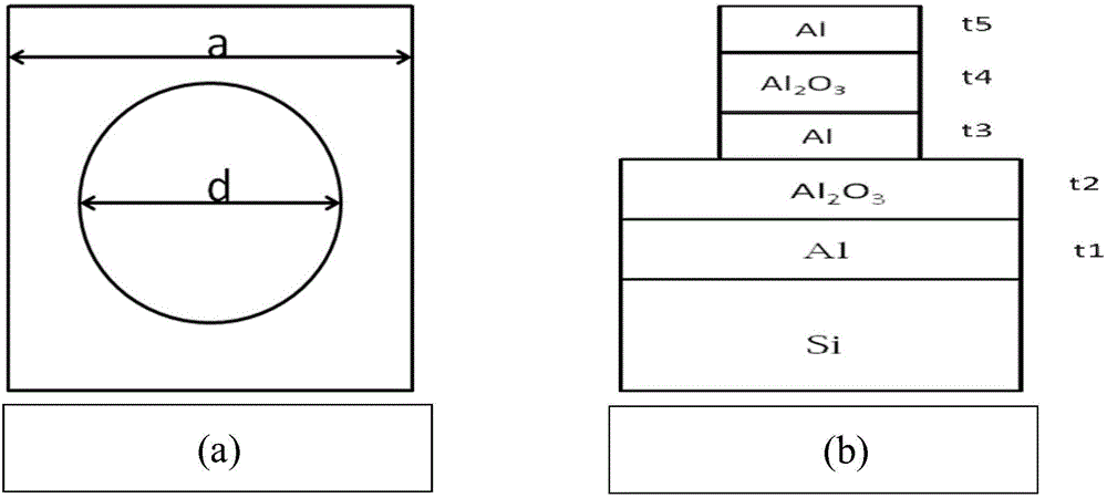
[0021] In the present invention, the wave-absorbing structure is designed on a substrate supported by Si, the bottom continuous metal film and metal layer are both Al, and the dielectric layer is Al 2 o 3 , a=6um, the diameter of the absorbing unit d=3.2um, the thickness of the first dielectric layer is 0.25um, the thickness of the second dielectric layer is 0.3um, the thickness of the metal layer is 0.1um, and the thickness of the underlying metal film is 200nm .
[0022] The parameters of reflectivity and transmittance were obtained through the commercial electromagnetic simulation software CSTMicrowaveStudio, and the absorption rate curve was calculated.
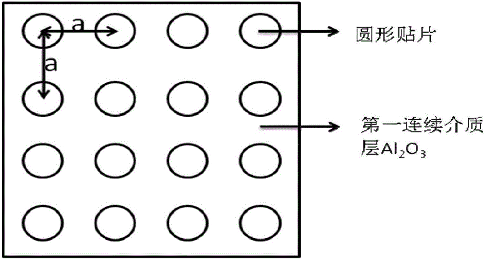
[0023] Use the center point of the circular patch as a reference. For a circular patch, the present invention uses its center-to-center distance as a reference for the row pitch and column pitch of the array. figure 1 (a) shows the average value range of each absorbing unit and the occupied bottom metal film and the fi...
PUM
| Property | Measurement | Unit |
|---|---|---|
| Center distance | aaaaa | aaaaa |
| Diameter | aaaaa | aaaaa |
| Thickness | aaaaa | aaaaa |
Abstract
Description
Claims
Application Information
 - R&D
- Intellectual Property
- Life Sciences
- Materials
- Tech Scout
- Unparalleled Data Quality
- Higher Quality Content
- 60% Fewer Hallucinations
Browse by: Latest US Patents, China's latest patents, Technical Efficacy Thesaurus, Application Domain, Technology Topic, Popular Technical Reports.
© 2025 PatSnap. All rights reserved.Legal|Privacy policy|Modern Slavery Act Transparency Statement|Sitemap|About US| Contact US: help@patsnap.com


