A photoelectric logic gate based on tin dioxide nanoparticles and its preparation method

A technology of tin dioxide and nanoparticles, applied in logic circuits using optoelectronic devices, logic circuits using specific components, logic circuits, etc., can solve problems such as incomplete functions of optoelectronic logic gates

Active Publication Date: 2017-07-18
HUAZHONG UNIV OF SCI & TECH
View PDF2 Cites 0 Cited by
  • Summary
  • Abstract
  • Description
  • Claims
  • Application Information

AI Technical Summary

Problems solved by technology

[0008] For the above defects or improvement needs of the prior art, the object of the present invention is a kind of optoelectronic logic gate based on tin dioxide nanoparticles and its preparation method, wherein through the structure of its key negative photoconductive device and its material, preparation Compared with the existing technology, it can effectively solve the problem of the incomplete function of the photoelectric logic gate, and the photoelectric logic gate can perform logic processing on simple optical signals to achieve the technical effect of stable operation.

Method used


Image

  • A photoelectric logic gate based on tin dioxide nanoparticles and its preparation method
  • A photoelectric logic gate based on tin dioxide nanoparticles and its preparation method
  • A photoelectric logic gate based on tin dioxide nanoparticles and its preparation method

Examples


Embodiment 1

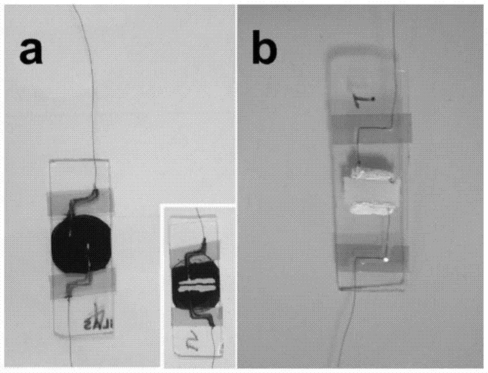
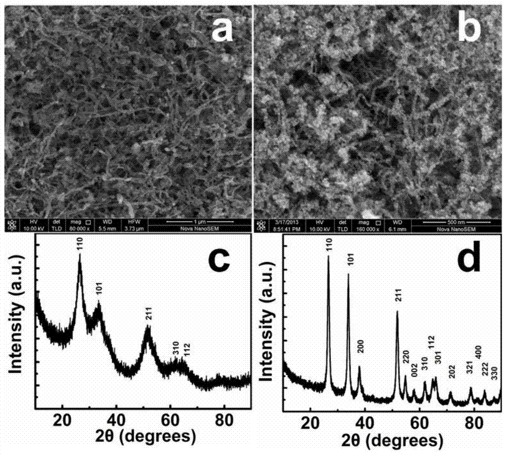
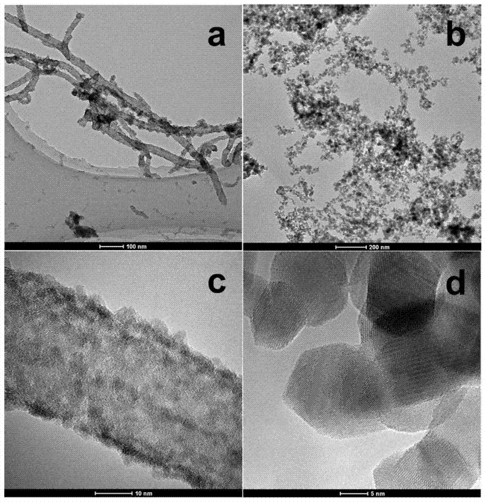
[0080] Both the negative photoconductive device and the positive photoconductive device in the present invention adopt an insulating substrate (such as a glass slide; because the input optical signal can directly irradiate on the material of the positive / negative photoconductive effect, such as tin dioxide nanoparticles, so the insulation The substrate is not required to be a light-transmitting insulating substrate) as the substrate, and the cost is low. Negative photoconductive devices use tin dioxide-coated carbon nanotube composites as working materials, which are easy to synthesize and make devices, and do not need to be packaged in vacuum or other harsh environments; positive photoconductive devices are simply annealed on the basis of negative photoconductive devices Only processing is required, the process is simplified and the cost is reduced. The negative photoconductive device and the positive photoconductive device are connected by copper wires to form a photoelectri...

Embodiment 2

[0100] Its preparation method of the optoelectronic logic gate based on tin dioxide nanoparticles in embodiment 2 is basically the same as embodiment 1, the difference is:

[0101] In step 1, the concentrated nitric acid volume that mass fraction is 65% is 30mL, and deionized water volume is 20mL, is made into the 40% nitric acid solution of 50mL;

[0102] In step 2, the quality of adding carbon nanotubes is 67 mg, and the stirring and reflux time of the solution is 8 hours;

[0103] In step 3, the obtained powder was dried at 70°C for 24 hours;

[0104] In step 4, the mass of stannous chloride dihydrate added is 0.45 g (i.e. 0.05 mol / L stannous chloride solution), the volume of 37% hydrochloric acid is 0.5 mL, and the mass of carbon nanotubes after drying is 8 mg;

[0105] In step 5, the temperature of the water bath is 50°C, and the duration is 4 hours;

[0106] In step 7, the silver paste pattern is 2mm×5mm, with a distance of about 0.1mm, and the annealing condition is 1...

Embodiment 3

[0111] Its preparation method of the optoelectronic logic gate based on tin dioxide nanoparticles in embodiment 3 is basically the same as embodiment 1, the difference is:

[0112] In step 1, mass fraction is that the concentrated nitric acid volume of 65% is 61mL, and ion water volume is 39mL, is made into the 40% nitric acid solution of 100mL;

[0113] In step 2, the quality of adding carbon nanotubes is 134 mg, and the stirring and reflux time of the solution is 12 hours;

[0114] In step 3, the obtained powder was dried at 90°C for 6 hours;

[0115] In step 4, the mass of stannous chloride dihydrate added is 1.36 grams (i.e. 0.15 mol / L stannous chloride solution), the volume of 37% hydrochloric acid is 1 mL, and the mass of carbon nanotubes after drying is 12 mg;

[0116] In step 5, the temperature of the water bath is 70°C, and the duration is 2 hours;

[0117] In step 7, the silver paste pattern is 2mm×8mm, with a distance of about 0.5mm, and the annealing condition is...


PUM

PropertyMeasurementUnit
lengthaaaaaaaaaa
thicknessaaaaaaaaaa
thicknessaaaaaaaaaa

Abstract

The invention discloses a photoelectric logic door based on stannic oxide nano-particles and a preparation method of the photoelectric logic door. The photoelectric logic door comprises a first positive photoconductive device and a first negative photoconductive device which are used cooperatively and for receiving a first optical signal, wherein the first positive photoconductive device adopts the stannic oxide nano-particles, the first negative photoconductive device adopts the stannic oxide / carbon nanotube composite material, both the first positive photoconductive device and the first negative photoconductive device are provided with an energy-supply electrode and an output electrode, the output electrode of the first positive photoconductive device is connected with that of the first negative photoconductive device, an end port is used for outputting the logic operation result, and the logic operation result is influenced by the first optical signal. The photoelectric logic door based on the stannic oxide nano-particles utilizes the negative photoconductive effect of the stannic oxide / carbon nanotube composite material, improves the response rate of the negative photoconductive device, and enables the function of the photoelectric logic door formed by the negative photoconductive device and an ordinary positive photoconductive device to be complete.

Description

technical field [0001] The invention belongs to the field of nanomaterial sensing, and more specifically relates to a photoelectric logic gate based on tin dioxide nanoparticles and a preparation method thereof. The photoelectric logic gate based on tin dioxide nanoparticles is specifically composed of tin dioxide nanoparticles and tin dioxide-coated carbon nanotube composite materials to form a positive photoconductive device and a negative photoconductive device, respectively. Background technique [0002] The rapid development of information technology has prompted more and more fields of computer, communication and control to use optical signals for transmission. All-optical devices that follow optical principles have been extensively studied, and all logic functions can be realized and integrated. On the other hand, whether it is a computer, a communication or a control terminal, all work with electrical signals, so it is necessary to quickly and effectively convert opt...

Claims


Application Information

Patent Timeline
Patent Type & Authority Patents(China)
IPC IPC(8): G02F3/00
CPCG02F3/00G02F2202/36
Inventor 高义华丁龙伟刘逆霜李露颖
Owner HUAZHONG UNIV OF SCI & TECH
Why Eureka
Try Eureka