Circuit board design method for portable terminal

A technology of a portable terminal and a design method, applied in the design field of terminal circuit boards, can solve the problems of multiple PCB area, large terminal size, unsuitable for carrying, and inconvenient for users to use, so as to reduce the size, ensure the performance and effect, and improve the experience. effect of effect

Active Publication Date: 2015-03-04
BEIJING HUATAI NOVA TECH
View PDF3 Cites 0 Cited by
  • Summary
  • Abstract
  • Description
  • Claims
  • Application Information

AI Technical Summary

Problems solved by technology

When designing its circuit board, the antenna has the requirement of clearance area, and the so-called clearance area means that there should be no metal devices or circuit traces in this part of the circuit board area, because they will affect the transmission and reception of the antenna. The quality affects the use effect of the terminal
However, usually for portable devices, there are requirements for test points or software debugging interfaces. These test points or debugging interfaces are relatively large and will take up a lot of PCB area, resulting in the entire terminal being too large to carry. User-friendly

Method used


Image

  • Circuit board design method for portable terminal
  • Circuit board design method for portable terminal

Examples


Embodiment Construction

[0016] The present invention will be further described in detail below in conjunction with the accompanying drawings, so that those skilled in the art can implement it with reference to the description.

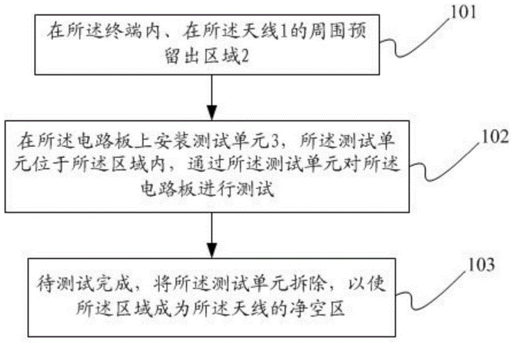
[0017] Such as Figure 1-2 As shown, the present invention provides a circuit board design method for a portable terminal, the terminal has an antenna for sending and receiving signals, and the antenna is installed on the circuit board, which includes:

[0018] Step 101, reserve an area 2 around the antenna 1 in the terminal;

[0019] Step 102, installing a test unit 3 on the circuit board, the test unit is located in the area, and the circuit board is tested by the test unit;

[0020] Step 103, after the test is completed, the test unit is removed, so that the area becomes a clear area of ​​the antenna. From figure 2 It can be seen that the test unit 3 is only set in the area to the left of the antenna on the circuit board, and there are no task metal parts and wiring in...


PUM


Abstract

The invention discloses a circuit board design method for a portable terminal. The terminal comprises an antenna for receiving and transmitting signals, wherein the antenna is mounted on a circuit board. The method includes the steps: reserving an area in the terminal and on the periphery of the antenna; mounting a testing unit on the circuit board; detaching the testing unit after testing and enabling the area to be a clear area of the antenna. The testing unit is positioned in the area and used for testing the circuit board. The testing unit occupying too much area of the circuit board is arranged in the clear area of the antenna, the clear area of the antenna cannot be affected when the testing unit is removed after testing, and the use performance of the whole terminal can be ensured after testing.

Description

technical field [0001] The invention relates to the field of circuit board design, in particular to a design method of a terminal circuit board with antenna design. Background technique [0002] Currently, for many portable terminals, an antenna for sending and receiving signals is indispensable. When designing its circuit board, the antenna has the requirement of clearance area, and the so-called clearance area means that there should be no metal devices or circuit traces in this part of the circuit board area, because they will affect the transmission and reception of the antenna. The quality further affects the use effect of the terminal. However, usually for portable devices, there are requirements for test points or software debugging interfaces. These test points or debugging interfaces are relatively large and will take up a lot of PCB area, resulting in the entire terminal being too large to carry. Inconvenient for users to use. Contents of the invention [0003...

Claims


Application Information

Patent Timeline
Patent Type & Authority Applications(China)
IPC IPC(8): H01Q1/24H01Q1/38
Inventor 袁丁
Owner BEIJING HUATAI NOVA TECH
Why Eureka
Try Eureka