Wafer tensioning device for semiconductor packaging

A technology for semiconductors and stretch sheets, which is used in the manufacture of semiconductor/solid-state devices, electrical components, circuits, etc., can solve the problems of inability to use metal wafer changing rings, inaccurate chip positions, uneven wafer stretching, etc., to achieve the operation process. Stable and reliable, the disc stretches evenly, and the structure is simple

Inactive Publication Date: 2014-03-05
NANTONG HUALONG MICROELECTRONICS
View PDF3 Cites 0 Cited by
  • Summary
  • Abstract
  • Description
  • Claims
  • Application Information

AI Technical Summary

Problems solved by technology

This type of stretcher structure not only takes up manpower, but also increases the process. At the same time, because the stretcher ring is a plastic structure, the metal change ring commonly used in the field of semiconductor packaging bonding cannot be used. In addition, the stretcher structure can only be used at most. 5-inch wafers are produced, larger than 5 inches, such as 6-inch wafers cannot be operated; at the same time, the existing stretcher device is easy to slide during the operation process, resulting in uneven stretching of the wafer and insufficient chip placement Accurate and other defects

Method used


Image

  • Wafer tensioning device for semiconductor packaging
  • Wafer tensioning device for semiconductor packaging
  • Wafer tensioning device for semiconductor packaging

Examples


Embodiment Construction

[0017] The present invention will be further described below with reference to the accompanying drawings and specific embodiments.

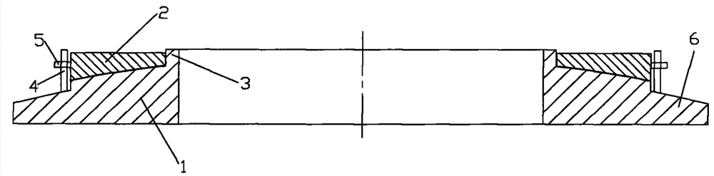
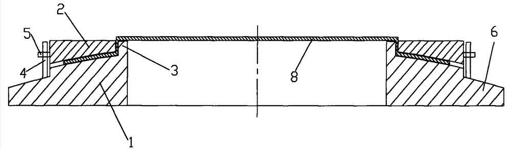
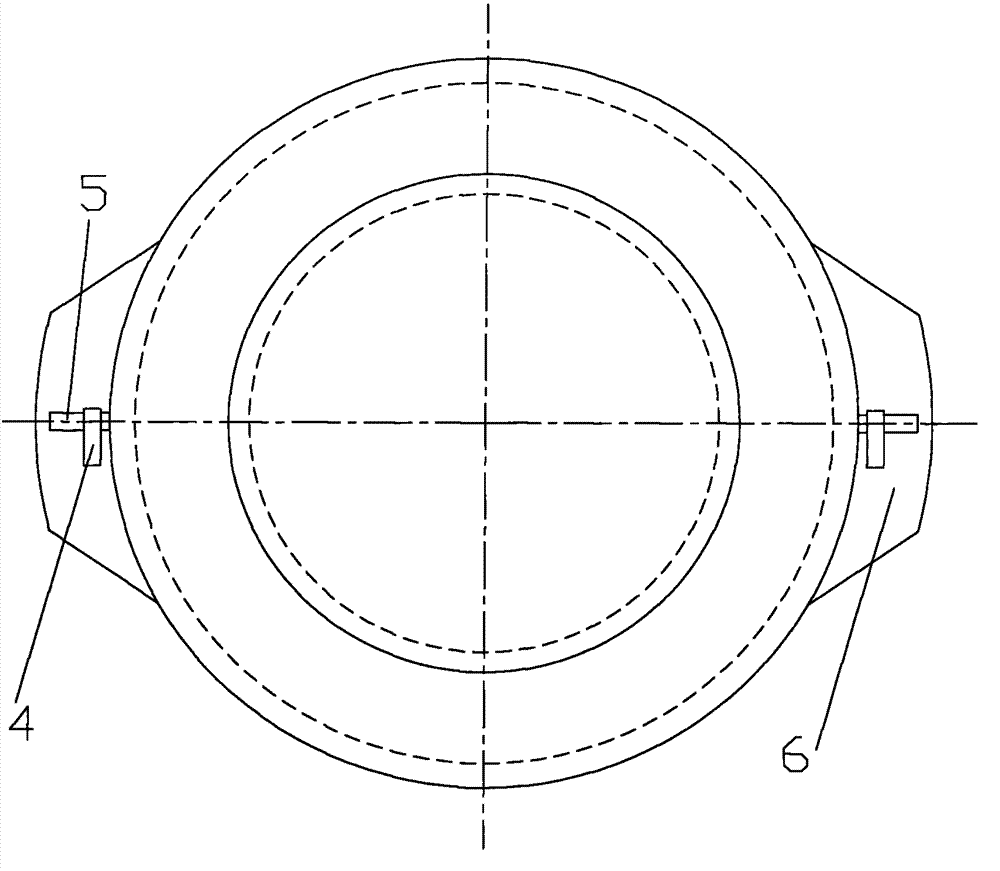
[0018] Such as figure 1 , figure 2 , image 3 as well as Figure 4 Shown: a stretcher device for semiconductor packaging according to an embodiment of the present invention, comprising a stretcher base 1 and a lower cover plate 2, a first cavity is provided inside the stretcher base 1, and a first cavity is arranged on the stretcher base 1 A stretcher-carrying convex ring 3 is provided, and a second cavity is arranged inside the stretcher-carrying convex ring 3, and the diameter of the second cavity is the same as that of the first cavity, and the stretcher-carrying convex ring 3 is provided with a second cavity. The outer diameter of the ring 3 is smaller than the outer diameter of the stretcher base 1, and the stretcher carrying convex ring 3 is used to support the scribe ring 8, and the scribe ring is provided with a disc; the lower cover ...


PUM


Abstract

The invention relates to a wafer tensioning device for semiconductor packaging. The wafer tensioning device for semiconductor packaging comprises a wafer tensioning base and a downward-pressing cover plate, wherein a first cavity is formed inside the wafer tensioning base, a wafer tensioning bearing protruding ring is arranged on the wafer tensioning base, a second cavity is formed inside the wafer tensioning bearing protruding ring, the diameter of the second cavity is equal to that of the first cavity, the outer diameter of the wafer tensioning bearing protruding ring is smaller than that of the wafer tensioning base, the downward-pressing cover plate is connected with the wafer tensioning base through a hinge, and is used in cooperation with the wafer tensioning base, a third cavity is formed inside the downward-pressing cover plate, the diameter of the third cavity is larger than the outer diameter of the wafer tensioning bearing protruding ring, and the downward-pressing cover plate is arranged on the wafer tensioning bearing protruding ring in a sleeved mode through the third cavity. The wafer tensioning device for semiconductor packaging has the advantages of being simple in structure, safe, reliable, high in working efficiency and wide in range of wafer tensioning.

Description

technical field [0001] The invention relates to a stretch sheet device for semiconductor packaging. Background technique [0002] In the semiconductor packaging die bonding process, the stretcher structure is a very important hardware configuration on the die bonding equipment. The integrity of the stretcher structure plays a leading role in the efficiency and quality of the die bonding. [0003] In the traditional stretcher device, the wafer of the chip must be expanded through the wafer expansion structure before use. When expanding, first fix the disk in two embedded plastic rings, then place the rings in the expansion structure of the disk, and then stick the disk. This type of stretcher structure not only takes up manpower and increases the process, but at the same time, because the stretcher ring is a plastic structure, the metal changer ring commonly used in the field of semiconductor packaging bonding cannot be used. In addition, the stretcher structure can only 5-...

Claims


Application Information

Patent Timeline
Patent Type & Authority Applications(China)
IPC IPC(8): H01L21/67
CPCH01L21/67092H01L21/68
Inventor 吴斌
Owner NANTONG HUALONG MICROELECTRONICS
Why Eureka
Try Eureka