
Silicon slice automatic slice counting method based on electronic balance

A technology of electronic balance and silicon wafer, which is applied in the direction of measuring devices, instruments, weighing, etc.

Active Publication Date: 2014-11-12
ZHEJIANG COWIN ELECTRONICS
View PDF4 Cites 0 Cited by
  • Summary
  • Abstract
  • Description
  • Claims
  • Application Information

AI Technical Summary

Problems solved by technology

[0006] In the actual production process, especially in the shipment inspection process, the check of the number of pieces is very important. The traditional manual spotting cannot meet the high requirements of the existing production for product quality. The photoelectric spotting machine is used in the semiconductor silicon wafer manufacturing industry. Apps have inherent flaws that cannot be avoided

Method used


Image

  • Silicon slice automatic slice counting method based on electronic balance
  • Silicon slice automatic slice counting method based on electronic balance
  • Silicon slice automatic slice counting method based on electronic balance

Examples


Embodiment 1

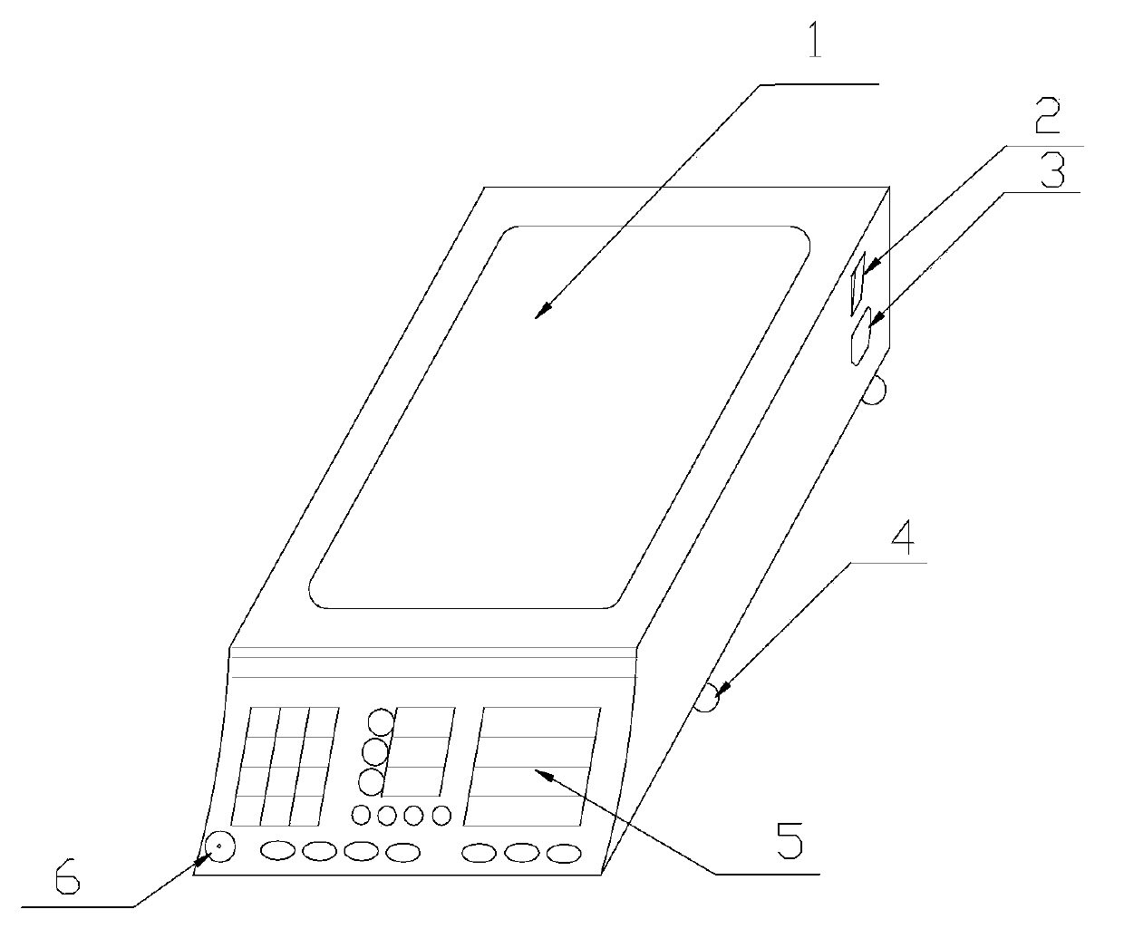
[0044] The actual use steps of the present invention: (with 285-290, 3-inch circular silicon wafers, 211pcs waiting for confirmation. According to the principle, the single maximum count n=56.)

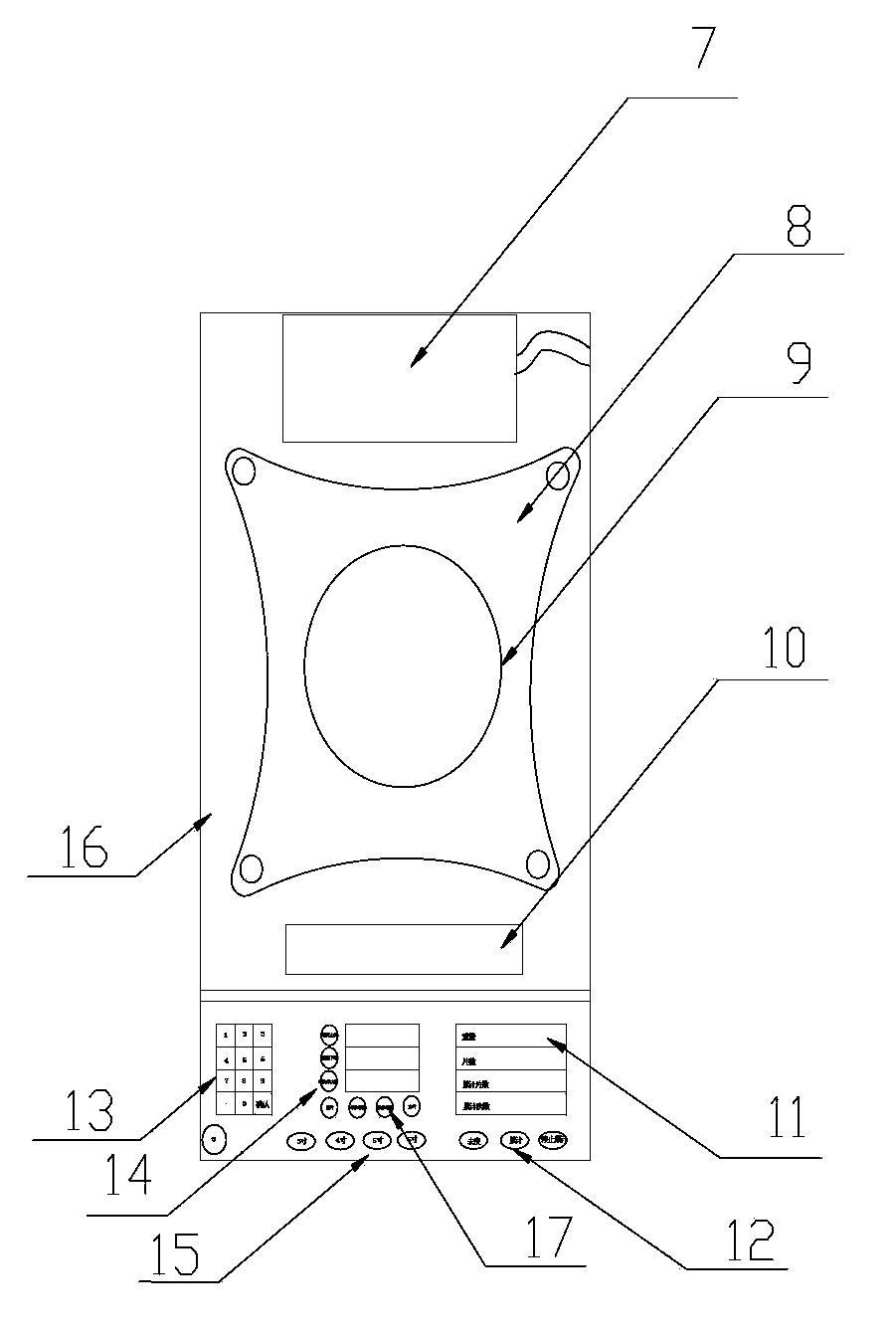
[0045] 1. Turn on the switch of the device, and place the basket containing silicon wafers on the balance.

[0046] 2. When the display is stable, click Tare.

[0047] 3. Place the test weight on the basket and confirm that the weight display is consistent with the weight identification.

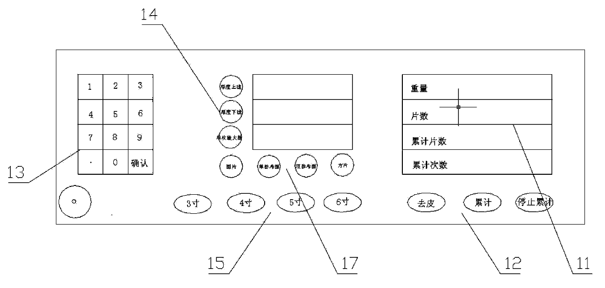
[0048] 4. Enter the silicon wafer thickness 285-290, and select "3 inches", "wafer".

[0049] 5. Put the wafers to be counted into the basket in batches, and click "Accumulate".

[0050] 6. If too many pieces are put in at one time, it will display "Exceeded" and will not be included in the cumulative number of pieces.

[0051] 7. Repeat steps 5-6 to get the final total number of pieces. Get "over", "56", "55", "over", "55", "45", respectively.

[0052] 8. "Accumulated number of pieces" display...

Embodiment 2

[0055] Shipment inspection, N14, 295-300 microns, 501pcs, wafers, 1pcs filter paper every 50pcs interval, of which 1 knife silicon wafer is 51pcs, the final inspection uses the device of the present invention for full inspection, and the final inspection requires 500pcs / box, 50pcs / Knife.

[0056] The inspection is as follows:

[0057] Testing frequency

Embodiment 3

[0059] 5-inch single reference surface, asymmetric chamfered silicon wafer, thickness 525-530 microns. The number of slices is unknown, and the number of slices is calculated using the device and method of the present invention.

[0060] 1. Input the upper and lower lines of the thickness to get the single maximum count value n=104pcs.

[0061] 2. Select the size "5 inches", "single reference plane", and press "cumulative" to count.

[0062] 3. Divided into multiple counts, respectively "52", "46", "68", "42", "45", a total of 253pcs.

[0063] 4. Checked by manual counting method, it is 253pcs, which is consistent with the result of the counting device.


PUM


Abstract

The invention discloses a silicon slice automatic slice counting method based on an electronic balance. The steps are as follows. Firstly, a choice is made for silicon slices which need to be weighted on a numerical value input device, a silicon slice thickness selecting and display device, a silicon slice specification selecting device and a silicon slice size selecting device. Secondly, an inner signal processing device disposes and figures out the number of slices of the silicon slice according to a weighting device, a silicon slice area calculating device, a silicon slice size calculating device and a silicon slice slice calculating device, and the number of the slices is shown on a calculating result display device. Based on a common electronic balance, the silicon slice automatic slice counting method based on the electronic balance mainly uses fixed physical property between weight and density to achieve slice calculation, is capable of achieving the slice calculation of the silicon slice, has the advantages of being convenient, practical and cheap.

Description

technical field [0001] The invention belongs to the field of semiconductor silicon wafer processing and manufacturing in the integrated circuit support industry, and in particular relates to an electronic balance-based automatic silicon wafer counting method, which is suitable for weighing and counting semiconductor silicon wafers. Background technique [0002] The semiconductor silicon wafer manufacturing industry belongs to the integrated circuit support industry. It has always been a key support industry and a strategic emerging industry. However, the statistics of the number of semiconductor silicon wafers have long been completed by manual spotting. Manual spotting is inevitable. Data errors will occur. In the semiconductor industry, which is an extremely rigorous field of production, the number of chips will greatly affect the product image; it will also have an adverse effect on the traceability of production data; loss. [0003] Photovoltaic industry is a rapidly de...

Claims


Application Information

Patent Timeline
Patent Type & Authority Patents(China)
IPC IPC(8): G01G19/42
Inventor 孙新利
Owner ZHEJIANG COWIN ELECTRONICS
Learn More