
Easily-debugged embedded system of complex SD (secure digital) interface

An embedded system, easy-to-debug technology, applied in the direction of instruments, electrical digital data processing, etc., can solve the problem of inconvenient debugging interface, and achieve the effect of convenient repair debugging and program upgrade process

Inactive Publication Date: 2015-05-27
SINO WEALTH ELECTRONICS
View PDF5 Cites 0 Cited by
  • Summary
  • Abstract
  • Description
  • Claims
  • Application Information

AI Technical Summary

Problems solved by technology

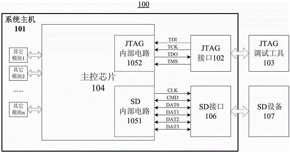
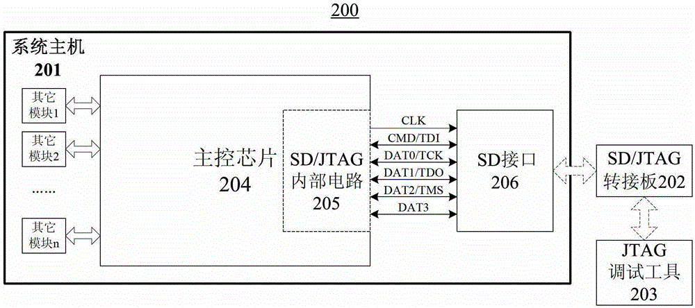
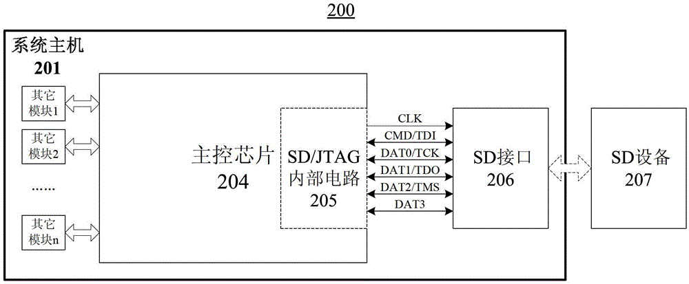
[0004] The technical problem to be solved by the present invention is to provide an easy-to-debug embedded system that reuses the SD interface, which can solve the problem of inconvenient access to the debug interface of embedded products, and greatly facilitates product repair and debugging and program upgrades

Method used


Image

  • Easily-debugged embedded system of complex SD (secure digital) interface
  • Easily-debugged embedded system of complex SD (secure digital) interface
  • Easily-debugged embedded system of complex SD (secure digital) interface

Examples


Embodiment Construction

[0022] The present invention will be further described below in conjunction with specific embodiment and accompanying drawing, set forth more details in the following description so as to fully understand the present invention, but the present invention can obviously be implemented in many other ways different from this description, Those skilled in the art can make similar promotions and deductions based on actual application situations without violating the connotation of the present invention, so the content of this specific embodiment should not limit the protection scope of the present invention.

[0023] The most commonly used debugging interface for embedded systems is the standard JTAG interface. The following will take the JTAG interface as an example to elaborate. JTAG is the abbreviation of the initials of the English "Joint Test Action Group (Joint Test Action Group)", which was established in 1985 and is a PCB and IC test standard initiated by several major electro...


PUM


Abstract

The invention provides an easily-debugged embedded system of a complex SD (secure digital) interface. The easily-debugged embedded system comprises a system main frame and an SD / debugging patch panel, wherein the system main frame comprises a main control chip and an SD interface, the main control chip is internally provided with an SD / debugging inner circuit; one end of the SD interface is connected with the SD / debugging inner circuit; and the SD / debugging patch panel is respectively connected with the other end of the SD interface and a debugging tool and is used for converting the SD interface into a debugging interface. The invention solves the problem that the debugging interface is guided out inconveniently, and a shell needs to be disassembled so that the efficiency is low and the shell is easy to break during disassembly in products of a main frame of a relatively applied embedded system when problem debugging or program updating is carried out through the debugging interface by utilizing a design method of multiplexing signal lines of the SD interface and the debugging interface, so that the great convenience can be provided for a product repair debugging and program updating process, and influences on the use experience of a user and the cost of a whole machine can be avoided.

Description

technical field [0001] The invention relates to the technical field of embedded systems, in particular, the invention relates to an easy-to-debug embedded system that multiplexes SD interfaces. Background technique [0002] In the existing embedded system (Embedded System), whether it is the early development of the main control chip or the subsequent maintenance of the whole system, the use of debugging tools is very important. When the main control chip is designed, there is usually a debugging interface for application development and debugging. After the whole machine system is confirmed to be mass-produced, the actual product will not lead out the debugging interface, because the user does not need to use it, and the corresponding interface will not be left on the product mold to avoid affecting the appearance. However, after the product is mass-produced, if there is a problem and you need to use the debugging tool to find the cause, you often need to open the product ...

Claims


Application Information

Patent Timeline
Patent Type & Authority Patents(China)
IPC IPC(8): G06F13/20
Inventor 余为国张钦张震生王磊
Owner SINO WEALTH ELECTRONICS
Learn More