
Design method of static random access memory suitable for low-power chip

A static random and design method technology, applied in static memory, digital memory information, information storage, etc., can solve the problems of rare circuit design methods, large load capacitance, large power consumption, etc., and reduce the charging and discharging power of word lines power consumption, improve stability, and reduce gate current

Inactive Publication Date: 2014-04-16
SHANGHAI JIAOTONG UNIV
View PDF3 Cites 0 Cited by
  • Summary
  • Abstract
  • Description
  • Claims
  • Application Information

AI Technical Summary

Problems solved by technology

[0008] In addition, there are a lot of transistors connected to the word line and the bit line in SRAM, and the load capacitance is large, so the power consumption generated by one charge and discharge is also large.
However, there are few circuit design methods to reduce word line power consumption.

Method used


Image

  • Design method of static random access memory suitable for low-power chip
  • Design method of static random access memory suitable for low-power chip
  • Design method of static random access memory suitable for low-power chip

Examples


Embodiment

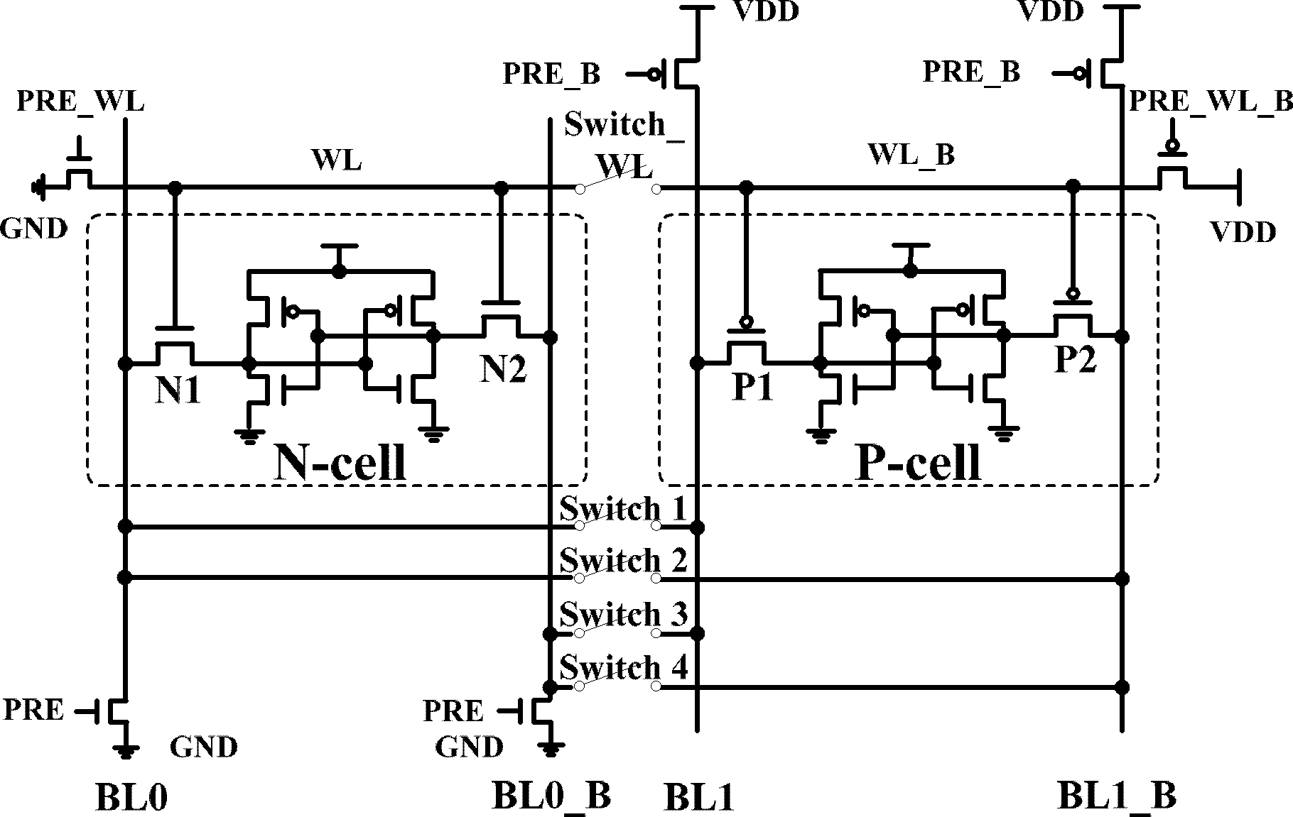
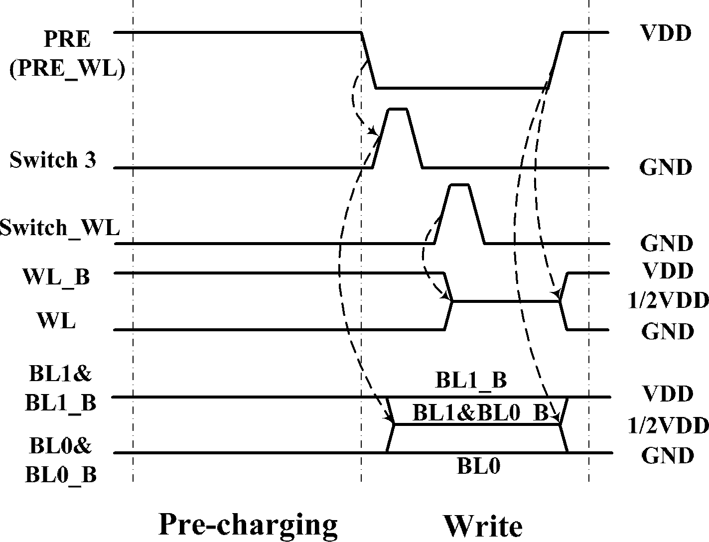
[0036] SRAM of the present invention is a circuit schematic diagram of a group of cell units composed of two different cells, such as figure 1shown. The bit lines BL0 and BL0_B are connected to GND through switches, and the bit lines BL1 and BL1_B are connected to VDD through switches. Four switches Switch1, Switch2, Switch3, and Switch4 control the connection between the bit lines, so that one bit line in the N-cell (or P-cell) can be connected to any one of the P-cell (or N-cell) Root bit line. For example, BL0 connects to BL1 through Switch1, and connects to BL1_B through Switch2. The data to be written is controlled by Switch1, Switch2, Switch3, and Switch4 to achieve the purpose of controlling the voltage difference of the bit lines, thereby writing the data into the inverter ring.

[0037] In the design of the word line, such as figure 1 shown. The access transistors N1, N2 and P1, P2 in the N-cell and P-cell are respectively controlled by two mutually opposite word...


PUM


Abstract

The invention relates to a design method of a static random access memory suitable for a low-power chip. The method comprises the following steps of: 1) executing bit line charge recycling on a bit line, namely, transferring the to-be released charges near by the bit line to the to-be-charged bit line beside, and reducing bit line charging-discharging power consumption by the charges on the bit line; 2) using uniform unit mechanism on a cell, namely, respectively using two cells with different structures in the same SRAM (Static Random Access Memory), and pre-charging the bit line of the cell to reach different voltage values while pre-charging so as to reduce the gate current power consumption in a hold mode; and 3) executing bit line charge recycling on the bit line, namely, controlling different cells by two reversed bit line signals, when gating, transferring the to-be-released charges on a non-WL-B signal to a bit line WL signal, namely, reducing the bit line charging-discharging power consumption again by the charges on the bit line. In comparison with the prior art, the method has the advantages of low power consumption, high stability and the like.

Description

technical field [0001] The invention relates to a design method of a static random access memory, in particular to a design method of a static random access memory suitable for low power consumption chips. Background technique [0002] Due to the rapid development of semiconductor chips, the functions of the chip are increasing day by day, and the processing capacity is continuously enhanced, which requires more and more high-performance caches to store instructions or temporary data during processing. This makes the on-chip cache composed of static random access memory (SRAM) larger and larger. According to statistics, in the processor chip, the area of ​​SRAM accounts for 80% of the entire chip area, or even more, and SRAM also consumes a large amount of memory simultaneously. power consumption. Especially in mobile handheld devices, the power consumption of SRAM has become one of the main factors limiting the application of the device. Reducing the power loss of SRAM ha...

Claims


Application Information

Patent Timeline
Patent Type & Authority Patents(China)
IPC IPC(8): G11C11/413
Inventor 王旭葛冰晶毛志刚
Owner SHANGHAI JIAOTONG UNIV
Learn More