Multilayer circuit board and assembly thereof

A multi-layer circuit board and circuit board technology, which is applied to printed circuits, printed circuit components, electrical components, etc., can solve the problems of ambiguous marking codes, unrecognizable reversed front and back, and inability to detect multi-layer circuit boards.

Inactive Publication Date: 2011-10-19
COMPEQ MFG
View PDF3 Cites 3 Cited by
  • Summary
  • Abstract
  • Description
  • Claims
  • Application Information

AI Technical Summary

Problems solved by technology

[0006] However, because an insulating layer is provided between the two circuit boards, because the material of the insulating layer is not completely transparent, the marking code of the circuit board closer to the bottom will become more and more blurred, which will cause the inspector to be unable to identify; moreover, the existing The slotting structure of the circuit board can only check whether there is a missing circuit board, but when the circuit board is misplaced, each identification code can still be revealed from the slots, and it is impossible to identify whether there is a reversed situation. The structure of the multi-layer circuit board still does not allow the inspector to check whether the multi-layer circuit board is placed correctly in order

Method used


Image

  • Multilayer circuit board and assembly thereof
  • Multilayer circuit board and assembly thereof
  • Multilayer circuit board and assembly thereof

Examples


Embodiment Construction

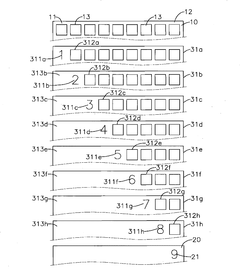
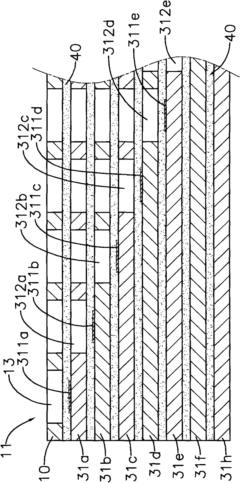
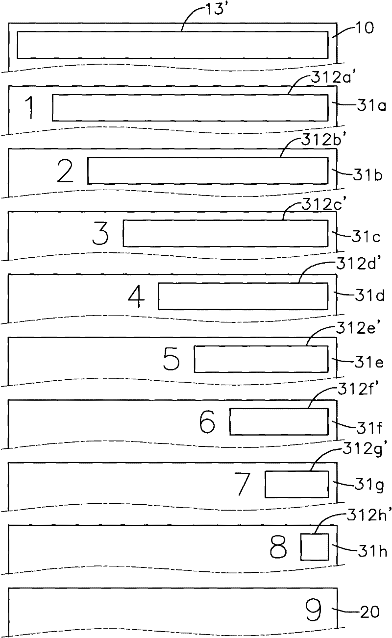
[0034] Please see figure 1 , figure 2 As shown, it is a multilayer circuit board of the first embodiment of the present invention, which includes:

[0035] A top outer layer circuit board (10), which is provided with n openings (13) at intervals from a first position (11) to an nth position (12) near an edge, where n is an integer greater than 2;

[0036] a bottom outer circuit board (20) forming an nth identification code (21) at an nth position (12) relative to the top outer layer circuit board (10);

[0037] a plurality of central circuit boards (31a-h) having n-1 central circuit boards (31a-h) from the top outer circuit board (10) towards the bottom outer circuit board (20), wherein the first central The circuit board (31a) is formed with a first identification code (311a) relative to the first position (11) of the top outer layer circuit board (10), and is spaced from the second position to the nth position (12) A plurality of first through holes (312a) are provided ...


PUM


Abstract

The invention discloses a multilayer circuit board, which comprises a top outer-layer circuit board, a bottom outer-layer circuit board, a plurality of central circuit boards and a plurality of insulating layers, wherein the top outer-layer circuit board is provided with n openings at intervals in a penetrating manner from the first position to the nth position at the position close to the edge; n is an integer greater than 2; the bottom outer-layer circuit board forms the nth marking code relative to the nth position the top outer-layer circuit board; the central circuit boards form marking codes in a steeped manner relative to the first position to the nth position of the top outer-layer circuit board; a plurality of penetration holes corresponding to the openings are arranged from the marking codes to the nth position; solid structures are arranged from the first position to the marking codes; and the insulating layers are arranged between the two circuit boards. By matching the solid structures of the central circuit boards with the penetrating structures, the accuracy of the arrangement of the central circuit boards can be detected easily.

Description

technical field [0001] The invention is a multilayer circuit board, especially a multilayer circuit board which is easy to check whether the stacking sequence is wrong. Background technique [0002] In response to the development of current technology, electronic equipment must have high-speed and large computing power and more complex functional applicability. Therefore, a single circuit board in electronic equipment is no longer enough. In order to increase the circuit density, multi-layer circuit boards are used. In many current electronic devices. [0003] The wiring area can be increased by stacking multilayer circuit boards. The multi-layer circuit board has an even number of layers, including a plurality of core boards composed of two-layer circuit boards and two outer-layer circuit boards arranged outside the core boards. An insulating layer is coated between each layer of circuit boards to press and bond each layer of circuit boards firmly, which means that an ins...

Claims


Application Information

Patent Timeline
Patent Type & Authority Applications(China)
IPC IPC(8): H05K1/00H05K1/02
Inventor 邱宏渝钟明宪吴侑霖
Owner COMPEQ MFG
Why Eureka
Try Eureka