Semiconductor device and method of manufacturing the same
A manufacturing method and semiconductor technology, applied in the direction of semiconductor/solid-state device manufacturing, semiconductor devices, electrical components, etc., can solve problems such as difficulty in realization, and achieve the effect of realizing terminal area, maintaining withstand voltage, and high withstand voltage
- Summary
- Abstract
- Description
- Claims
- Application Information
AI Technical Summary
Problems solved by technology
Method used
Image

Examples
Embodiment approach 1
[0071]
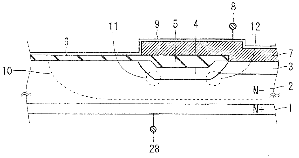
[0072] figure 1 It is a sectional view of the terminal region of the power device chip of the present invention, showing a PN junction structure. The structure of a diode is described here as an example of a device. The channel stop area and scribe lines are omitted for convenience.
[0073] On the surface of the low-concentration N-type drift layer 2 formed (epitaxially grown) on the high-concentration N-type substrate 1, the P base layer 3 as the active layer is diffused to form a P base layer 3 to surround the active unit of the P base layer 3 region (a diode is formed in this embodiment), a P well layer 4 is formed as a first well region. The P well layer 4 is the main junction portion of the guard ring structure, and is adjacent to the P base layer 3 and diffused into a ring shape. Further, in the P well layer 4 , along its ring shape, a trench region 5 (sinking region) is formed as a ring-shaped concave portion having a tapered shape whose side surfaces exp...
Embodiment approach 2
[0110]
[0111] In Embodiment 1, the diffusion depth of the P base layer 3 is shallower than the diffusion depth of the P well layer 4, but as Figure 9 As shown, both can be set to the same degree of diffusion depth. The other configurations are the same as those in Embodiment 1, and therefore detailed descriptions are omitted.
[0112]
[0113] By forming the P base layer 3 and the P well layer 4 in this way, the electric field is not concentrated on one radius of curvature portion 22 of the P well layer 4, and the breakdown caused by the avalanche breakdown of the radius of curvature portion 22 is less likely to occur. Improve pressure resistance.
[0114]
[0115] According to Embodiment 2 of the present invention, in the semiconductor device, the diffusion depth of the P base layer 3 as the active layer and the P well layer 4 as the first well region on the high-concentration N-type substrate 1 as the semiconductor substrate is Therefore, the electric field does n...
Embodiment approach 3
[0117]
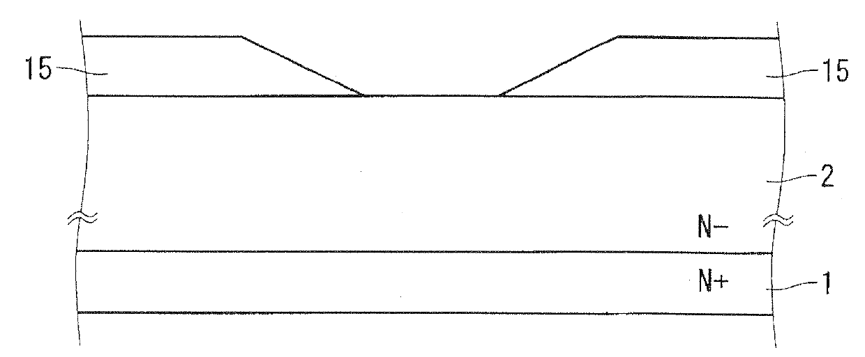
[0118] In Embodiment Mode 1, the trench region 5 having a tapered shape was formed by dry etching, but as Figure 10~Figure 13 As shown in the process, it can also be formed by the LOCOS (Local Oxidation of Silicon, local oxidation of silicon) oxidation process.
[0119] The following shows the LOCOS oxidation flow. first as Figure 10 As shown, a low-concentration N-type drift layer 2 is formed on a high-concentration N-type substrate 1 , and a nitride film 23 is used to form a pattern for forming a P well layer 4 on the low-concentration N-type drift layer 2 . Nitride film 23 is formed in a region other than the region to be P well layer 4 .
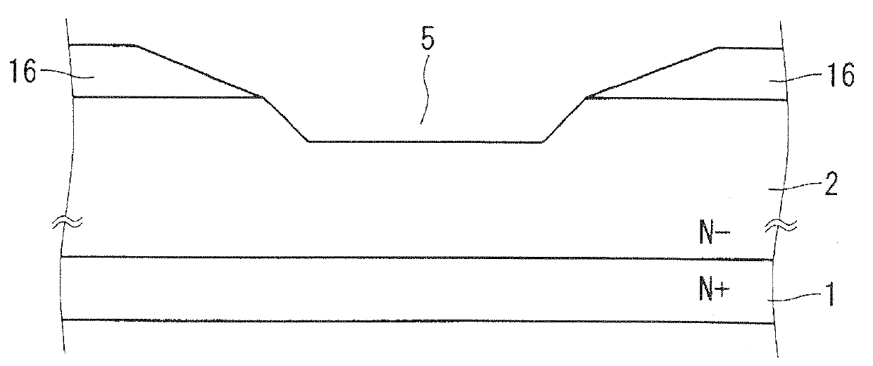
[0120] Then as Figure 11 As shown, the LOCOS oxide film 25 is formed by LOCOS oxidation. Then as Figure 12 As shown, the nitride film 23 and the LOCOS oxide film 25 are removed, and a photoresist 26 is formed so as to open the pattern to be the P well layer 4 . At this time, in the portion where the LOCOS oxide film ...
PUM
 Abstract
Description
Claims
Application Information
 - R&D
- Intellectual Property
- Life Sciences
- Materials
- Tech Scout
- Unparalleled Data Quality
- Higher Quality Content
- 60% Fewer Hallucinations
Browse by: Latest US Patents, China's latest patents, Technical Efficacy Thesaurus, Application Domain, Technology Topic, Popular Technical Reports.
© 2025 PatSnap. All rights reserved.Legal|Privacy policy|Modern Slavery Act Transparency Statement|Sitemap|About US| Contact US: help@patsnap.com