Alignment device for planar element, manufacturing equipment for the same, alignment method for the same, and manufacturing method for the same

A technology for manufacturing devices and alignment devices, which is applied in semiconductor/solid-state device manufacturing, photolithography on patterned surfaces, and instruments, and can solve problems such as increased cost on the device side and deterioration of accuracy

Inactive Publication Date: 2011-02-23
FUJITSU LTD
View PDF4 Cites 25 Cited by
  • Summary
  • Abstract
  • Description
  • Claims
  • Application Information

AI Technical Summary

Problems solved by technology

[0012] Therefore, a plurality of positioning marks are required to detect the orientation of the workpiece, and an additional camera or a moving mechanism for the camera is required to image

Method used


Image

  • Alignment device for planar element, manufacturing equipment for the same, alignment method for the same, and manufacturing method for the same
  • Alignment device for planar element, manufacturing equipment for the same, alignment method for the same, and manufacturing method for the same
  • Alignment device for planar element, manufacturing equipment for the same, alignment method for the same, and manufacturing method for the same

Examples


Embodiment Construction

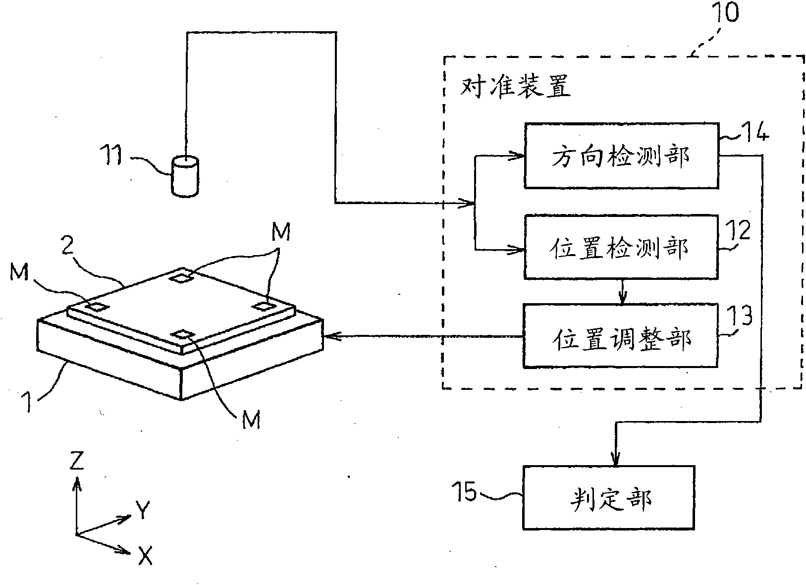
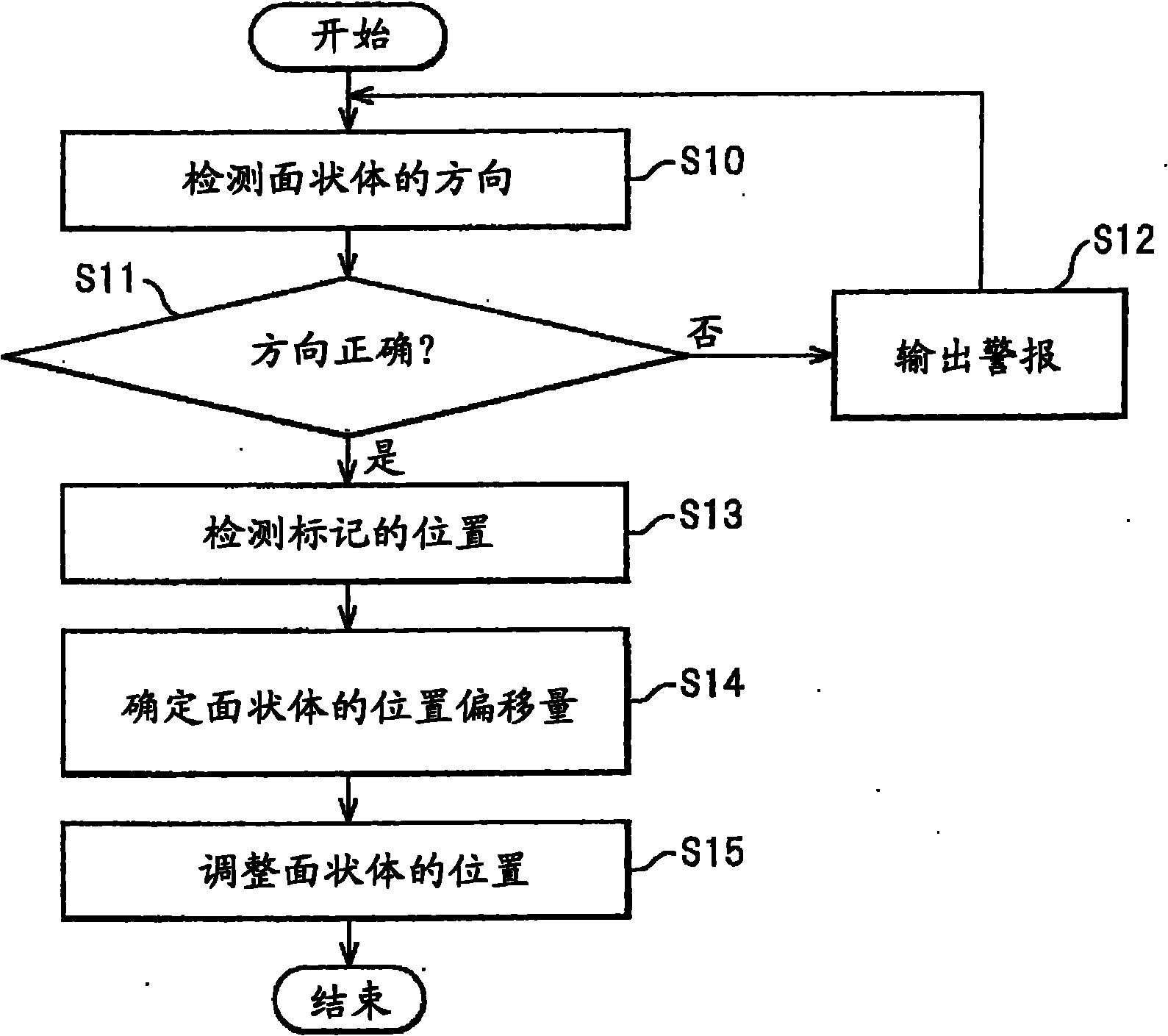
[0062] Hereinafter, embodiments of the present invention will be described with reference to the drawings. figure 1 is a block diagram of an embodiment of the alignment device. figure 1 is a block diagram of an embodiment of the alignment device. The alignment device 10 is a device for aligning a planar body 2 , which is a planar object such as a plate or a sheet, placed along the illustrated XY plane with respect to a predetermined reference position.

[0063] The alignment device 10 has: an imaging unit 11, which photographs a predetermined alignment mark M provided on the surface of the planar body 2; a position detection unit 12, which detects the position of the alignment mark M based on the image obtained by the imaging unit 11; position adjustment part 13, which adjusts the relative position between the reference position and the planar body 2 according to the position of the alignment mark M detected by the position detection part 12; The orientation of the planar bo...


PUM


Abstract

An alignment device (10) for a planar element (2) includes an imaging section (11) to image a picture of a non-rotational symmetry-shaped alignment mark M provided on the planar element (2), a position detection section (12) to detect a position of the alignment mark M from the image, a position adjustment section (13) to adjust a relative position of a specified reference position and the planar element (2) in accordance with a detected position of the alignment mark M, and an orientation detection section (14) to detect an orientation of the planar element (2) in accordance with the non-rotational symmetry of the alignment mark M imaged on a picture.

Description

technical field [0001] The present invention relates to the production process of transparent plates and sheets such as liquid crystal panels, electronic paper, organic EL (Electro-Luminescence: electroluminescence), or circuit boards and semiconductor integrated circuits. An apparatus and method for aligning a planar object such as a photomask used in a semiconductor integrated circuit manufacturing process. Background technique [0002] For plate-shaped objects, sheets, substrates, semiconductor In manufacturing equipment that handles planar workpieces such as wafers and planar components such as photomasks, the positions of these planar workpieces and components are automatically detected for alignment. For the sake of simplicity in the following description, workpieces such as plate-shaped objects, sheets, substrates, and semiconductor wafers, and members on the manufacturing apparatus side such as photomasks may be simply referred to as “workpieces”. [0003] The foll...

Claims


Application Information

Patent Timeline
IPC IPC(8): G03F1/00H01L21/027G03F9/00G03F1/42G03F1/84
CPCG03F1/14G03F1/144G03F9/7011H01L21/67092G03F9/7088G03F9/7076H01L21/681G03F1/00G03F1/36G03F1/42H01L21/0274
Inventor 原田徹三岛和久山西宏和
Owner FUJITSU LTD
Why Eureka
Try Eureka