


Quick Research
Generate reliable direction feasibility study reports for your R&D in just a few steps.

Technical Q&A
Discover and master advanced knowledge NOW. Basics, ideas, possibilities, all at once.

Find Solutions
As an expert in R&D theories, this can generate solutions to your technical problems instantly.

Evaluate Feasibility
Analyze your overall solution with one click, know your potential R&D risks in advance.

Monitor Landscape
Get weekly tech updates, stay abreast of the latest tech innovations and key insights.
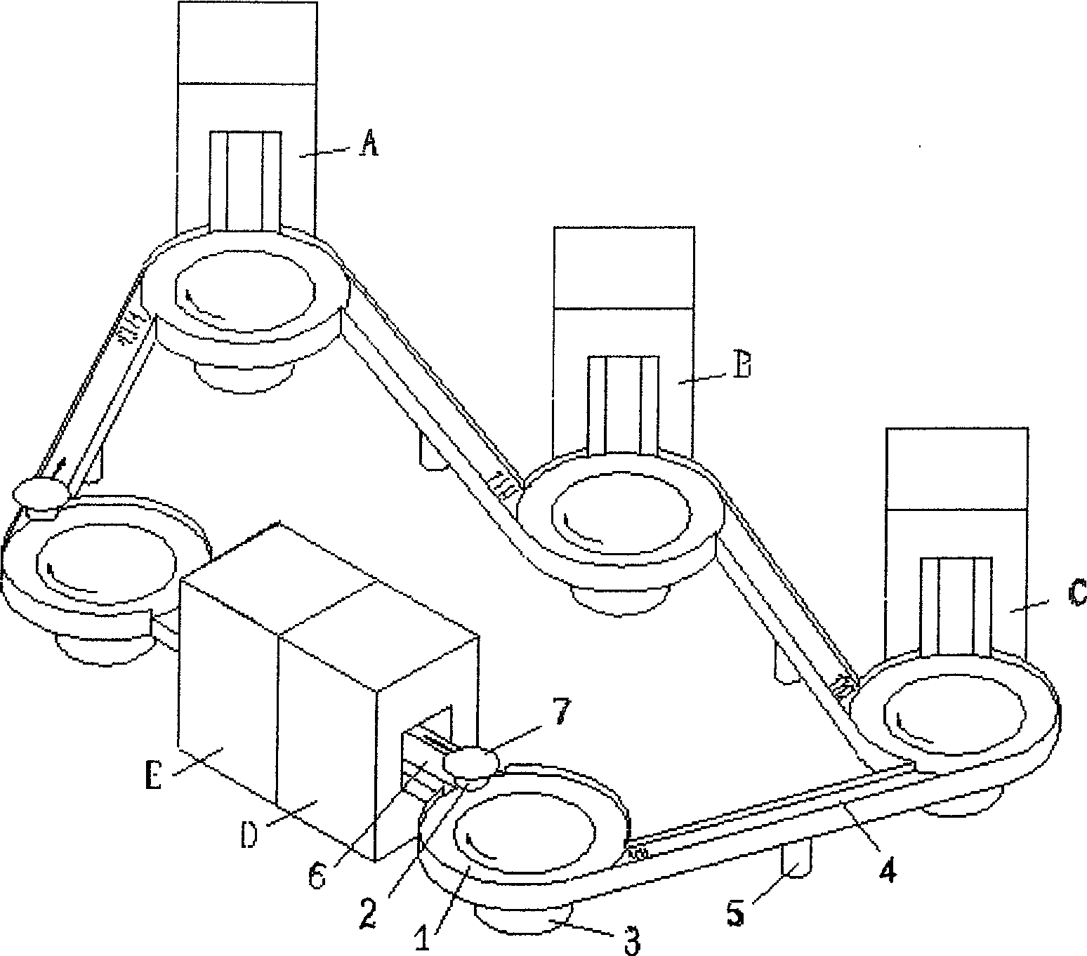
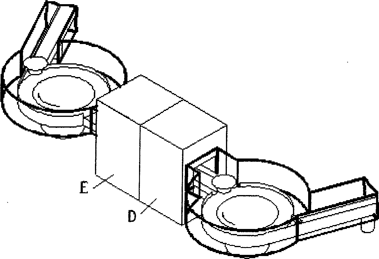
Silicon wafer high speed transport method and system capable of implementing multi-position processing
A high-speed transmission, multi-station technology, applied in the direction of conveyor objects, transportation and packaging, etc., can solve the problems of silicon wafer transmission robot research and development and manufacturing cost increases, achieve a good development space, reduce development costs, and reduce floor space Effect
- Summary
- Abstract
- Description
- Claims
- Application Information
AI Technical Summary
Problems solved by technology
Method used
Image

Examples
Embodiment 1
[0030] (a) Place the silicon wafer on the silicon wafer carrier and send the silicon wafer carrier to the turntable in the wafer output station, the movement radius of the silicon wafer carrier is 200mm;
[0031] (b) increasing the rotating speed of the turntable in the film output station to 72 rpm, so that the silicon wafer carrier can obtain a speed of 1.5m / s driven by the turntable in the film output station;
[0032] (c) The silicon wafer carrier enters the transfer track through the transfer interface between the turntable in the wafer output station and the transfer track, and moves toward the turntable in the first station at a speed of 1.5 m / s. The length of the transmission track horizontally arranged between the turntable in the film output station and the turntable in the first station is 1m, and the silicon wafer carrier is placed 0.25m before entering the turntable in the first station. The coefficient of friction with the transmission track is increased from 0.0...
Embodiment 2
[0035] (a) Place the silicon wafer on the silicon wafer carrier and send the silicon wafer carrier to the turntable in the wafer output station, the movement radius of the silicon wafer carrier is 200mm;
[0036] (b) The turntable in the film output station is accelerated to rotate to 144 rpm, so that the silicon wafer carrier can obtain a speed of 3m / s under the drive of the turntable in the film output station;
[0037](c) The silicon wafer carrier enters the transfer track through the transfer interface between the turntable in the wafer output station and the transfer track, and moves toward the turntable in the first station at a speed of 3 m / s. The length of the transmission track horizontally arranged between the turntable in the film output station and the turntable in the first station is 2m, and the silicon wafer carrier is placed 0.8m before entering the turntable in the first station. The coefficient of friction with the transmission track is increased from 0.05 to...
Embodiment 3
[0040] (a) Place the silicon wafer on the silicon wafer carrier and send the silicon wafer carrier to the turntable in the sheet output station, the movement radius of the silicon wafer carrier is 150mm;
[0041] (b) increasing the rotating speed of the turntable in the film output station to 76 rpm, so that the silicon wafer carrier can obtain a speed of 1.2m / s driven by the turntable in the film output station;
[0042] (c) The silicon wafer carrier enters the transfer track through the transfer interface between the turntable in the wafer output station and the transfer track, and moves toward the turntable in the first station at a speed of 1.2 m / s. The length of the transmission track arranged horizontally between the turntable in the film output station and the turntable in the first station is 0.8m, and the silicon wafer is carried at 0.15m before entering the turntable in the first station. The friction coefficient between the carrier and the transport track is increas...
PUM
 Abstract
Description
Claims
Application Information
 - R&D Engineer
- R&D Manager
- IP Professional
- Industry Leading Data Capabilities
- Powerful AI technology
- Patent DNA Extraction
Browse by: Latest US Patents, China's latest patents, Technical Efficacy Thesaurus, Application Domain, Technology Topic, Popular Technical Reports.
© 2024 PatSnap. All rights reserved.Legal|Privacy policy|Modern Slavery Act Transparency Statement|Sitemap|About US| Contact US: help@patsnap.com