Drive protection circuit, semiconductor module, and automobile
a protection circuit and semiconductor technology, applied in the direction of electronic switching, pulse technique, transportation and packaging, etc., can solve the problem of adverse influence on the switching element, and achieve the effect of reliably suppressing the surge voltag
- Summary
- Abstract
- Description
- Claims
- Application Information
AI Technical Summary
Benefits of technology
Problems solved by technology
Method used
Image
Examples
first embodiment
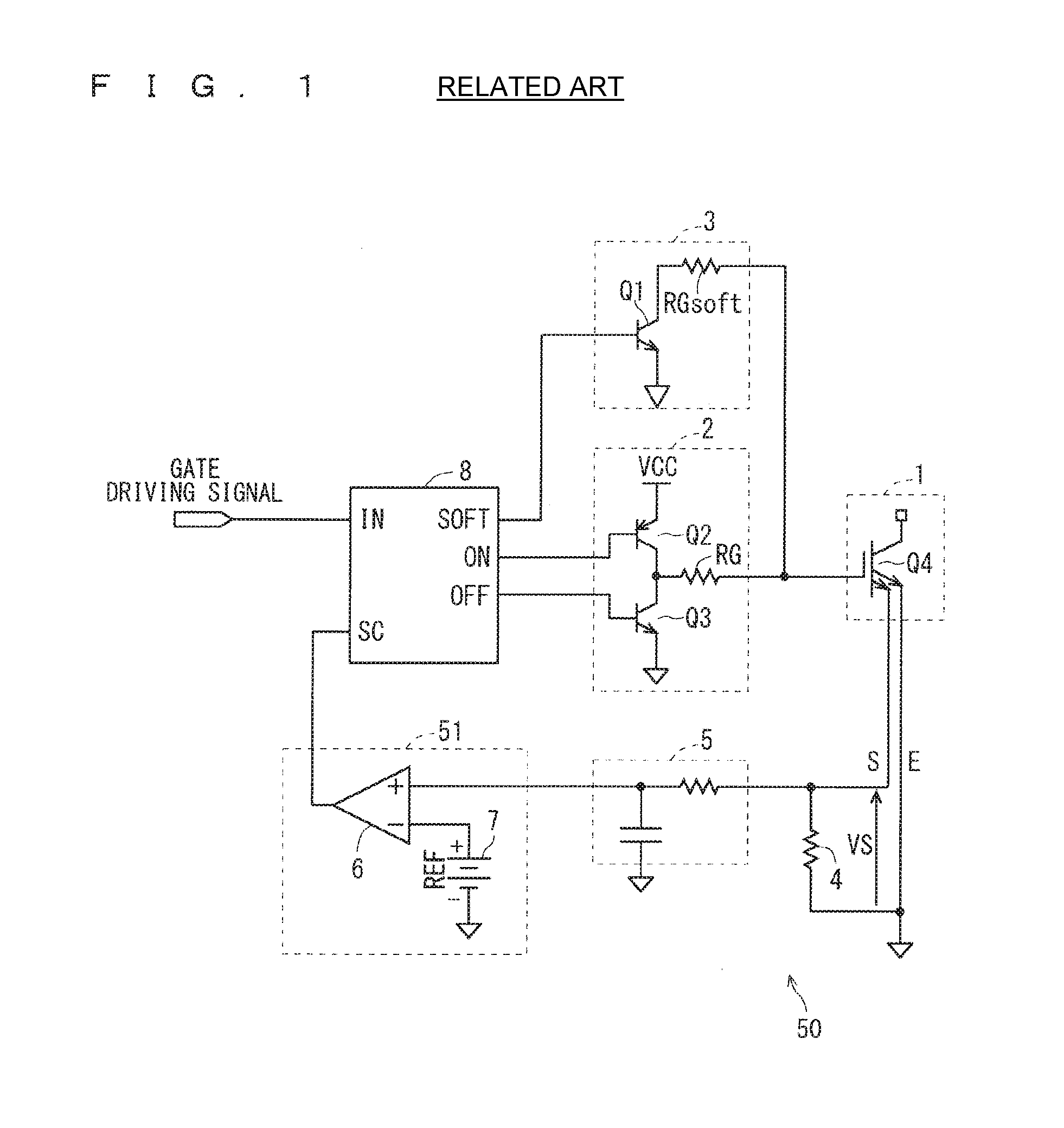
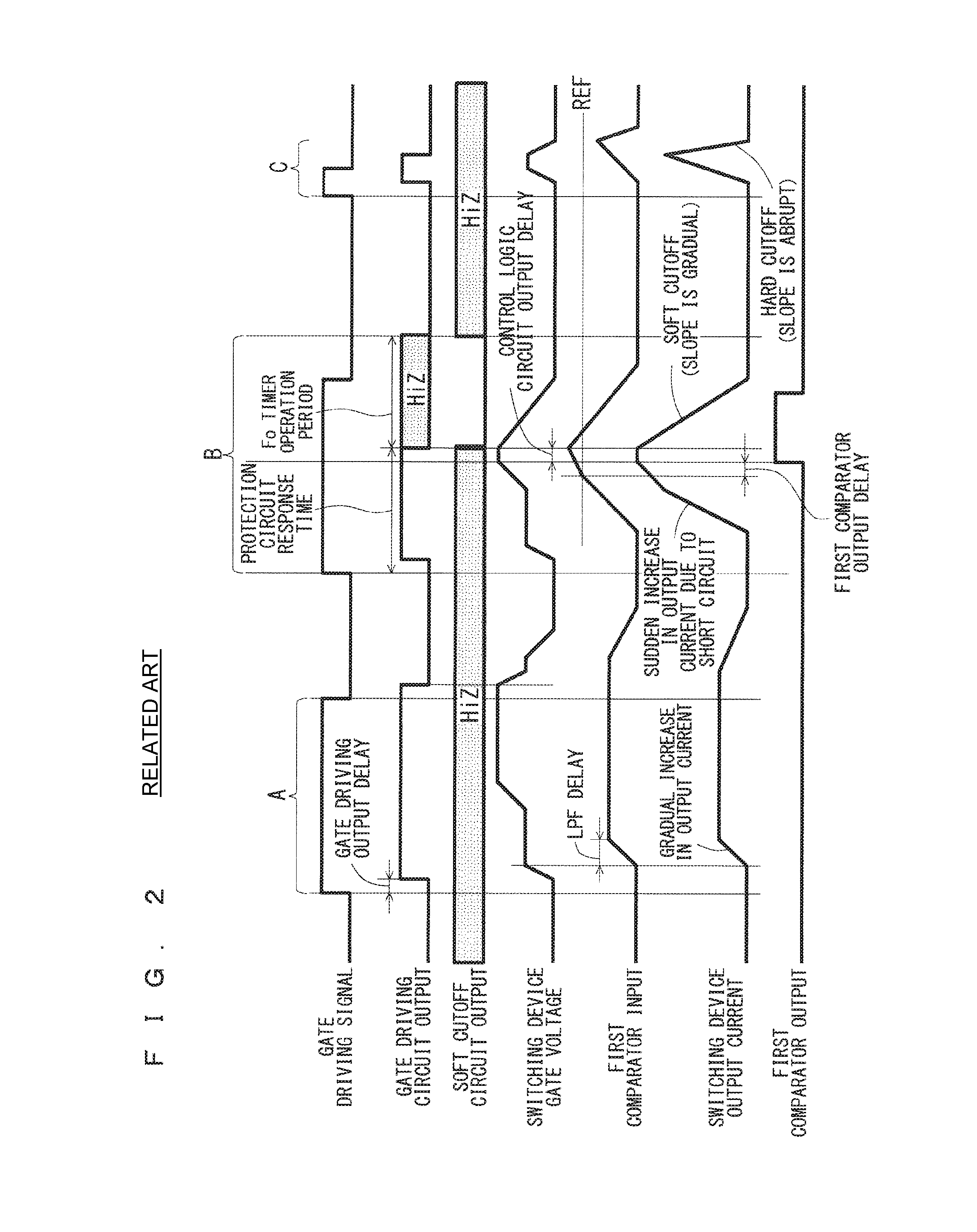
[0031]First, prior to description of a drive protection circuit according to a first embodiment of the present invention, a drive protection circuit related to that (hereinafter referred to as a “related drive protection circuit”) will be described. FIG. 1 is a circuit diagram illustrating a configuration of the related drive protection circuit, and FIG. 2 is a diagram illustrating an operation timing of the related drive protection circuit.
[0032]The related drive protection circuit is a circuit that drives and protects a switching element Q4 of a switching device 1 and is configured to include, as shown in FIG. 1, a gate driving circuit (drive circuit) 2, a soft cutoff circuit 3, a sense resistor 4, a low pass filter (LPF) 5, a first comparator 6, a power supply 7 having a reference voltage REF, and a control logic circuit 8 collectively controlling these.
[0033]Among these structural components, the structural components except for the above-mentioned gate driving circuit 2 (namely...
second embodiment
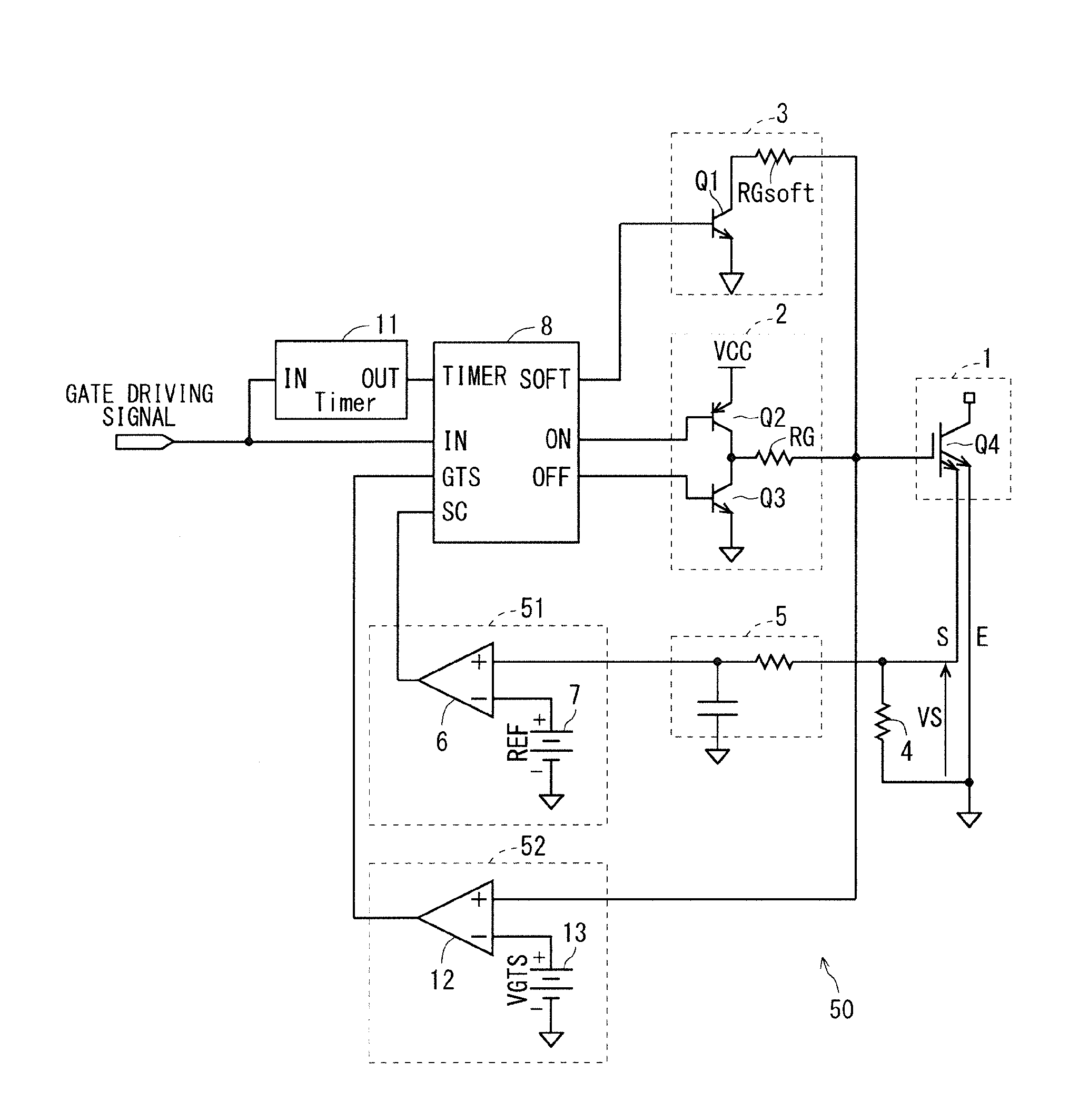
[0100]FIG. 14 is a circuit diagram illustrating a configuration of a drive protection circuit according to a second embodiment of the present invention, and FIG. 15 is a diagram illustrating an operation timing of the drive protection circuit. In the drive protection circuit according to the second embodiment, the same components as or similar components to those described in the first embodiment are denoted by the same references, and differences are mainly described below.
[0101]The drive protection circuit according to the second embodiment is the drive protection circuit according to the first embodiment as shown in FIG. 8 provided with a third comparator 16 and a power supply 17 having a reference voltage Vmirror, instead of the timer circuit 11.
[0102]In the drive protection circuit according to the second embodiment having such configuration, a mirror period of the switching element Q4 is used instead of the response time of the overcurrent protection circuit 50 as described ab...
third embodiment
[0109]FIG. 18 is a circuit diagram illustrating a configuration of a drive protection circuit according to a third embodiment of the present invention, and FIG. 19 is a diagram illustrating an operation timing of the drive protection circuit. In the drive protection circuit according to the third embodiment, the same components as or similar components to those described in the first embodiment are denoted by the same references, and differences are mainly described below.
[0110]The drive protection circuit according to the third embodiment is the drive protection circuit according to the first embodiment shown in FIG. 8 in which the timer circuit 11 receives the gate voltage of the switching element Q4 instead of the gate driving signal.
[0111]In the drive protection circuit according to the third embodiment having such configuration, a period of time (hereinafter “rise-to-off time”) from rising of the gate voltage of the switching element Q4a to turning OFF the gate driving signal i...
PUM
 Abstract
Description
Claims
Application Information
 - R&D
- Intellectual Property
- Life Sciences
- Materials
- Tech Scout
- Unparalleled Data Quality
- Higher Quality Content
- 60% Fewer Hallucinations
Browse by: Latest US Patents, China's latest patents, Technical Efficacy Thesaurus, Application Domain, Technology Topic, Popular Technical Reports.
© 2025 PatSnap. All rights reserved.Legal|Privacy policy|Modern Slavery Act Transparency Statement|Sitemap|About US| Contact US: help@patsnap.com


