Method for manufacturing semiconductor device

a manufacturing method and semiconductor technology, applied in the direction of semiconductor devices, electrical devices, transistors, etc., can solve the problems of adverse effects on the characteristics of transistors, inability to obtain sufficient characteristics with conventional techniques, and inability to manufacture sufficient characteristics, etc., to achieve convenient operation, excellent current characteristics, and easy operation

Inactive Publication Date: 2010-10-05
SEMICON ENERGY LAB CO LTD
View PDF11 Cites 4 Cited by
  • Summary
  • Abstract
  • Description
  • Claims
  • Application Information

AI Technical Summary

Benefits of technology

[0026]In the case of using a transistor as a switch, polarity (a conductivity type) of the transistor is not particularly limited because it operates just as a switch. However, a transistor of polarity with smaller off-current is preferably used when off-current is to be suppressed. Examples of a transistor with smaller off-current are a transistor provided with an LDD region, a transistor with a multi-gate structure, and the like. In addition, it is preferable that an N-channel transistor be used when a potential of a source terminal is closer to a potential of a low-potential-side power supply (e.g., Vss, GND, or 0 V), while a P-channel transistor be used when the potential of the source terminal is closer to a potential of a high-potential-side power supply (e.g., Vdd). This is because the absolute value of gate-source voltage can be increased when the potential of the source terminal is closer to a potential of a low-potential-side power supply in an N-channel transistor and when the potential of the source terminal is closer to a potential of a high-potential-side power supply in a P-channel transistor, so that the transistor can be more precisely operated as a switch. This is also because the transistor does not often perform a source follower operation, so that reduction in output voltage does not often occur.
[0093]A large semiconductor device or a large display device can be manufactured. Alternatively, a semiconductor device which easily operates normally or a display device which easily operates normally can be manufactured. Further alternatively, a semiconductor device having excellent current characteristics or a display device having excellent current characteristics can be manufactured.

Problems solved by technology

However, in the case where an SOI substrate is formed by bonding a single-crystal silicon layer to a glass substrate which is used in a liquid crystal panel or the like for cost reduction of the substrate, there is a problem in that heat treatment at such a high temperature causes a warp in the glass substrate.
In addition, there is also a problem in that strain stress is applied to the single-crystal silicon layer, so that characteristics of the transistor are adversely affected.
That is, even when a single-crystal silicon layer is provided over a glass substrate and a transistor is manufactured using the single-crystal silicon layer, sufficient characteristics cannot be obtained with the conventional technique.
In this case, it is difficult to arrange the plurality of semiconductor substrates over the glass substrate with accurate alignment.

Method used


Image

  • Method for manufacturing semiconductor device
  • Method for manufacturing semiconductor device
  • Method for manufacturing semiconductor device

Examples


embodiment mode 1

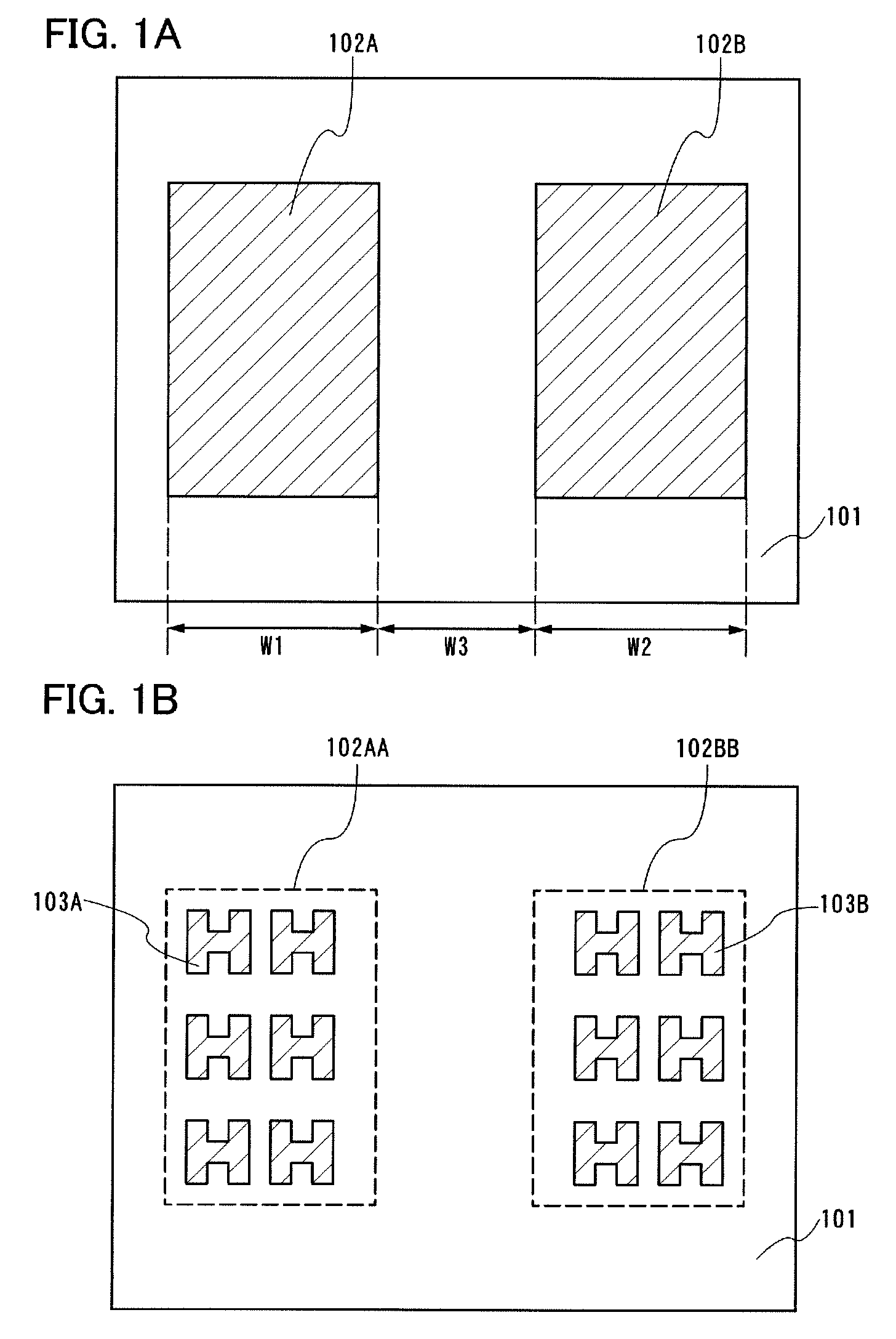
[0135]All or part of a semiconductor device or a display device is formed using a TFT which is formed over an insulating substrate by extracting a single-crystal semiconductor layer from a single-crystal semiconductor substrate and fixing the single-crystal semiconductor layer to the insulating substrate, or a TFT which is formed over an insulating substrate by attaching a single-crystal semiconductor substrate to the insulating substrate and fixing a single-crystal semiconductor layer which is part of the single-crystal semiconductor substrate to the insulating substrate by separating the single-crystal semiconductor substrate. Note that a TFT which is formed over an insulating substrate by extracting a single-crystal semiconductor layer from a single-crystal semiconductor substrate and fixing the single-crystal semiconductor layer to the insulating substrate, or a TFT which is formed over an insulating substrate by attaching a single-crystal semiconductor substrate to the insulati...

embodiment mode 2

[0159]In this embodiment mode, an example is shown in which arrangement which is different from that in Embodiment Mode 1 is performed.

[0160]FIGS. 4A and 4B show the case where four single-crystal semiconductor layers are provided. Note that the number of single-crystal semiconductor layers is not limited to four. As shown in FIG. 4A, a single-crystal semiconductor layer 402A and a single-crystal semiconductor layer 402B, which are displaced obliquely, are provided over the insulating substrate 101.

[0161]Note that a lower-right portion of the single-crystal semiconductor layer 402A in the diagram and an upper-left portion in the single-crystal semiconductor layer 402B in the diagram are closely provided. Note that the present invention is not limited to this. The lower-right portion of the single-crystal semiconductor layer 402A in the diagram and the upper-left portion in the single-crystal semiconductor layer 402B in the diagram may be spaced apart from each other.

[0162]Here, the ...

embodiment mode 3

[0208]Next, a method for manufacturing a single-crystal TFT is described.

[0209]FIGS. 14A and 14B show an SOI substrate of the present invention. In FIG. 14A, a base substrate 1400 is a substrate having an insulating surface or an insulating substrate, and any of various glass substrates which are used in the electronics industry, such as aluminosilicate glass substrates, aluminoborosilicate glass substrates, and barium borosilicate glass substrates can be used. Alternatively, a quartz glass substrate or a semiconductor substrate such as a silicon wafer can be used. An SOI layer 1402 is a single-crystal semiconductor, and single-crystal silicon is typically used. Alternatively, a single-crystal semiconductor layer formed of silicon, germanium, or a compound semiconductor such as gallium arsenide or indium phosphide which can be separated from a single-crystal semiconductor substrate by a separation method of hydrogen ion implantation can be used.

[0210]Between the base substrate 1400 ...


PUM


Abstract

To provide a method for manufacturing a large semiconductor device which easily operates normally and has excellent current characteristics. A first single-crystal semiconductor layer is provided over an insulating substrate. Then, the first single-crystal semiconductor layer is processed into an island shape. After that, a second single-crystal semiconductor layer is provided over the insulating substrate so as to overlap with part of a region where the first single-crystal semiconductor layer is provided. After that, the second single-crystal semiconductor layer is processed into an island shape. Thus, defects at joint portions in the case of providing the single-crystal semiconductor layers can be reduced.

Description

BACKGROUND OF THE INVENTION[0001]1. Field of the Invention[0002]The present invention relates to a device and a manufacturing method thereof. In particular, the present invention relates to a manufacturing method of a display device or a semiconductor device. Specifically, the present invention relates to a manufacturing method of a display device or a semiconductor device, in which a single-crystal semiconductor is fixed to an insulating substrate.[0003]2. Description of the Related Art[0004]In recent years, a technique for forming a thin film transistor (TFT) by using a semiconductor thin film (having a thickness of approximately several to several hundreds of nanometers) formed over a substrate having an insulating surface has attracted attention. Thin film transistors have been widely applied to electronic devices such as ICs and electro-optical devices and have been rapidly developed particularly as switching elements for image display devices.[0005]In order to obtain high-defi...

Claims


Application Information

Patent Timeline
Patent Type & Authority Patents(United States)
IPC IPC(8): H01L21/762H01L21/02H01L21/336H01L27/12H01L29/786
CPCH01L27/1214H01L27/1266H01L29/66772H01L27/1225H01L27/1277
Inventor KIMURA, HAJIME
Owner SEMICON ENERGY LAB CO LTD
Why Eureka
Try Eureka