Programmable logic device graph drawing method and device
A technology of programming logic and graphic rendering, applied in instruments, special data processing applications, electrical digital data processing, etc., can solve the problems of poor user experience satisfaction, unfavorable designer design, lack of overall sense, etc., and achieves low display level, Conducive to design and avoids the effect of overall feeling
- Summary
- Abstract
- Description
- Claims
- Application Information
AI Technical Summary
Problems solved by technology
Method used
Image
Examples
Embodiment 1
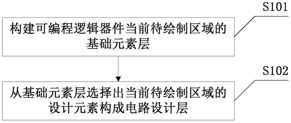
[0071] In this embodiment, according to the display level, the modification frequency, and the number of updated objects, the programmable logic device is designed in a priority hierarchy, and it is first divided into a basic element layer containing all basic elements and a circuit design layer containing all related elements; wherein The basic element layer has a low display level, low modification frequency, and a large number of update objects, so it is the underlying base layer; on the contrary, the circuit design layer has a high display level, high modification frequency, and a small number of update objects. on the outermost layer. Based on this layered idea, see figure 1 As shown, the programmable logic device graphics drawing method provided in this embodiment includes:
[0072] Step 101: Construct the basic element layer of the current area to be drawn in the programmable logic device;
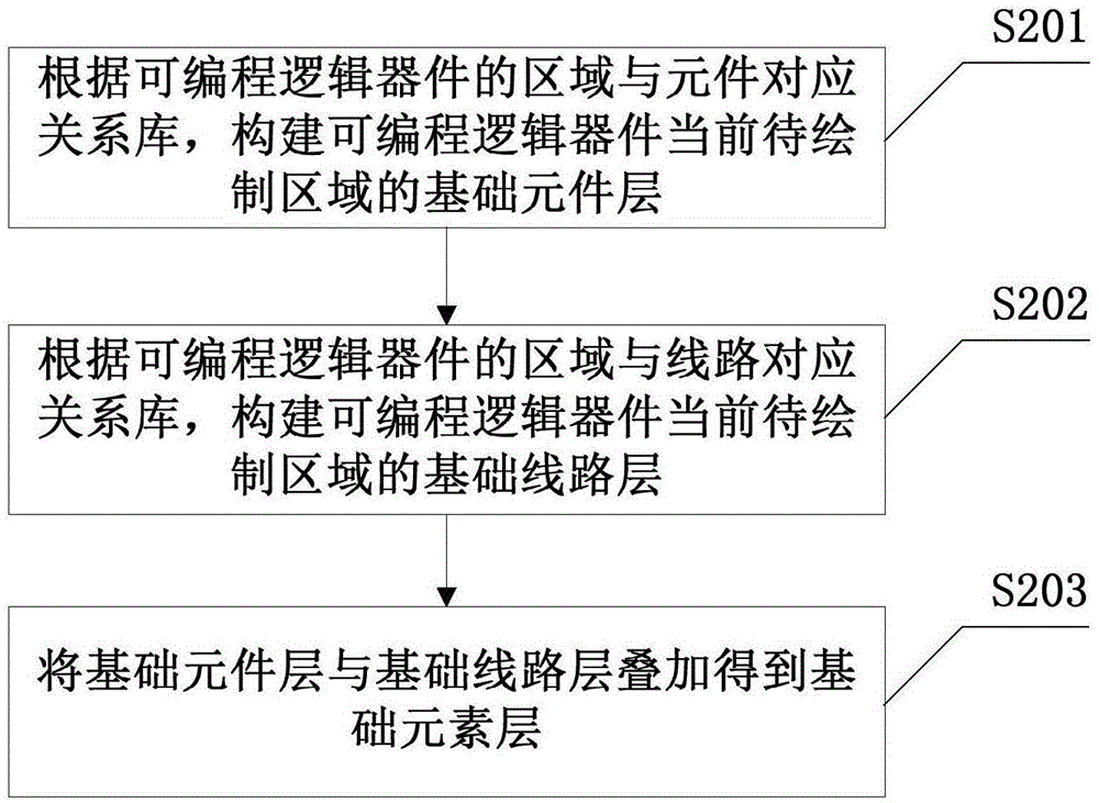
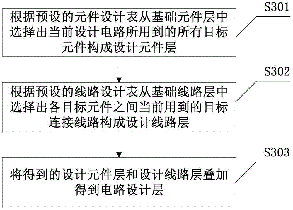
[0073] The basic element layer constructed here includes all elements in the ...
Embodiment 2
[0101] See Figure 5 As shown, this embodiment provides a programmable logic device graphics drawing device, including:
[0102] The basic element layer building module is used to construct the basic element layer of the current area to be drawn of the programmable logic device, and the basic element layer includes all elements of the current area to be drawn of the programmable logic device and all connection lines between the elements;
[0103] The circuit design layer construction module is used to select the design elements of the current area to be drawn of the programmable logic device from the basic element layer to form the circuit design layer; the design elements include the current design circuit used in the current area to be drawn of the programmable logic device All target elements and the currently used target connection lines between each target element.
[0104] Specifically, see Figure 6 As shown, the basic element layer construction module in this embodim...
Embodiment 3
[0121] For a better understanding of the present invention, this embodiment takes the application of the solution provided by the present invention to EDA to realize the drawing of FPGA diagram as an example to further illustrate the present invention.
[0122] Targeted for FPGA. In the hierarchical model, each level is prioritized according to the three dimensions of display level, modification frequency, and the number of updated objects. If the display level is high, the modification frequency is high, and the number of updated objects is small, it will be drawn at the top of the hierarchical model, and vice versa. The bottom layer of the model is drawn. To operate the interface, you only need to delete, redraw and superimpose one or several layers as needed.
[0123] For the FPGA layered model, please refer to Figure 10 Shown: FGPA is abstracted into a 5-layer model, sorted according to the display priority of different objects and the refresh frequency that needs to be...
PUM
 Abstract
Description
Claims
Application Information
 - R&D
- Intellectual Property
- Life Sciences
- Materials
- Tech Scout
- Unparalleled Data Quality
- Higher Quality Content
- 60% Fewer Hallucinations
Browse by: Latest US Patents, China's latest patents, Technical Efficacy Thesaurus, Application Domain, Technology Topic, Popular Technical Reports.
© 2025 PatSnap. All rights reserved.Legal|Privacy policy|Modern Slavery Act Transparency Statement|Sitemap|About US| Contact US: help@patsnap.com


