Organic electroluminescent device and display device

An electroluminescent device and electroluminescent technology, which are applied in the direction of electric solid devices, electrical components, semiconductor devices, etc., can solve the problems of reducing the output light efficiency of OLED light-emitting devices, and achieve the effect of improving the output light efficiency.

Active Publication Date: 2016-12-14
BOE TECH GRP CO LTD
View PDF7 Cites 0 Cited by
  • Summary
  • Abstract
  • Description
  • Claims
  • Application Information

AI Technical Summary

Problems solved by technology

[0003] However, in OLED light-emitting devices, different structures have differences in refractive index due to different materials, so that most of the light is totally reflected at the interface between different structures and cannot be exported. figure 1 It is a schematic structural diagram of an OLED light-emitting device in the prior art. The OLED light-emitting device includes an array substrate and a packaging substrate 2', and the array substrate includes a base substrate 1', an anode layer 4', a pixel definition layer (PDL) 3', and a cathode layer 6' and the organic light-emitting layer 5' between the anode layer 4' and the cathode layer 6', the light emitted by the organic light-emitting layer 5' is emitted through the packaging substrate 2', however, because the refractive index of the packaging substrate 2' is greater than that of the outside air Refractive index, so that part of the light incident on the interface cannot exit through the packaging substrate 2' due to total reflection, thereby reducing the output light efficiency of the OLED light emitting device

Method used


Image

  • Organic electroluminescent device and display device
  • Organic electroluminescent device and display device
  • Organic electroluminescent device and display device

Examples


Embodiment Construction

[0025] The specific implementation manners of the present invention will be further described in detail below in conjunction with the accompanying drawings and embodiments. The following examples are used to illustrate the present invention, but are not intended to limit the scope of the present invention.

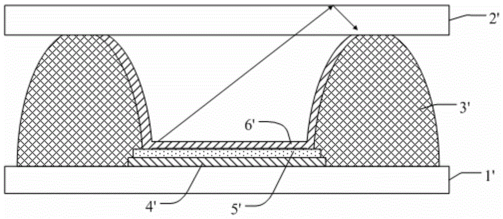
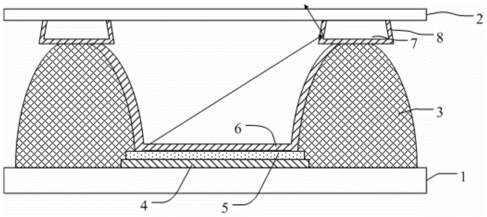
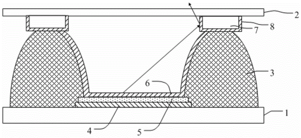
[0026] figure 2 It is a schematic diagram of an organic electroluminescent device provided in an embodiment of the present invention, the organic electroluminescent device includes an array substrate and a packaging substrate 2, and the array substrate includes a base substrate 1, an anode layer 4, and a pixel definition layer (PDL) 3 , the cathode layer 6 and the organic light-emitting layer 5 between the anode layer 4 and the cathode layer 6, wherein a protrusion 7 formed of a first transparent material is provided on the side of the packaging substrate facing the array substrate, the The surface of the protrusion 7 is also covered with a transparent layer 8 formed of ...


PUM


Abstract

The present invention provides an organic electroluminescent device and a display device. The organic electroluminescent device includes an array substrate and a package substrate, and the side of the package substrate facing the array substrate is provided with a protrusion formed of a first transparent material. , the raised surface is further covered with a transparent layer formed of a second transparent material having a higher refractive index than the first transparent material. In the present invention, a protrusion is provided on the side of the packaging substrate facing the array substrate, and a transparent layer with a refractive index greater than that of the protrusion is formed on the surface of the protrusion. When the light emitted by the organic light-emitting layer irradiates the surface of the protrusion, due to The refractive index of the protrusion is smaller than that of the transparent layer, so that part of the light irradiated on the convex surface is totally reflected to change the optical path, reducing the incident light that is totally reflected at the interface between the packaging substrate and the external air, and making the light after changing the optical path It is easier to emit light through the packaging substrate, thereby improving the output light efficiency of the OLED light-emitting device.

Description

technical field [0001] The invention relates to the display field, in particular to an organic electroluminescence device and a display device. Background technique [0002] Organic electroluminescent devices (OLEDs) are considered to have great application prospects in flat-panel displays because of their self-luminescence, all-solid-state, wide viewing angle, and fast response. A new generation of flat panel display products. [0003] However, in OLED light-emitting devices, different structures have differences in refractive index due to different materials, so that most of the light is totally reflected at the interface between different structures and cannot be exported. figure 1 It is a schematic structural diagram of an OLED light-emitting device in the prior art. The OLED light-emitting device includes an array substrate and a packaging substrate 2', and the array substrate includes a base substrate 1', an anode layer 4', a pixel definition layer (PDL) 3', and a cat...

Claims


Application Information

Patent Timeline
Patent Type & Authority Patents(China)
IPC IPC(8): H01L51/50H01L51/52H01L27/32
CPCH10K59/10H10K50/84H10K50/858H10K59/122H10K50/844H10K50/00H10K50/80H10K59/00
Inventor 许晓伟龙春平石磊徐文清
Owner BOE TECH GRP CO LTD
Why Eureka
Try Eureka