
Multilayer circuit board with high mechanical drilling yield and manufacturing method thereof

A multi-layer circuit and mechanical drilling technology, applied in the direction of multi-layer circuit manufacturing, printed circuit manufacturing, printed circuit, etc., can solve the problems of increasing production cost, increasing false positive rate, time-consuming and laborious, etc., and improving drilling qualification efficiency, improve production efficiency

Active Publication Date: 2017-02-01
SHENZHEN HUALIN CIRCUIT TECH
View PDF4 Cites 0 Cited by
  • Summary
  • Abstract
  • Description
  • Claims
  • Application Information

AI Technical Summary

Problems solved by technology

[0012] 1) The average value of expansion and contraction is calculated by using a small sampling method. Due to the difference in the expansion and contraction coefficient of the materials of the boards with less coverage, it will lead to an increase in the misjudgment rate, so that more errors will be generated when drilling via holes. Defective products with open circuit or short circuit
[0013] 2) If the expansion and shrinkage value of the circuit board is measured by the second dimension for the whole batch of multi-layer circuit boards, it will be time-consuming and laborious, which will greatly increase the production cost

Method used


Image

  • Multilayer circuit board with high mechanical drilling yield and manufacturing method thereof
  • Multilayer circuit board with high mechanical drilling yield and manufacturing method thereof
  • Multilayer circuit board with high mechanical drilling yield and manufacturing method thereof

Examples


Embodiment Construction

[0042] The multilayer circuit board with high mechanical drilling yield of the present invention can be a multilayer rigid-flex board or a multilayer flexible circuit board.

[0043] Multilayer circuit board of the present invention is made according to the following steps:

[0044] 1) Before laminating at least one layer of hard board made of FR-4 epoxy glass fiber board or No-Flow PP board and at least one layer of soft board made of PI material according to the method of the prior art, the multiple Select a layer of preset soft boards that have been routed in the first layer of circuit boards.

[0045] 2) Making the same original drill tape as the circuit on the preset flexible board, provided with via holes for the circuit to be drilled.

[0046] 3) On the original drill tape, 3-5 identification holes (not identified in the figure) with the same diameter as the circuit conduction hole are arranged staggeredly, and the position of the identification hole corresponds to the...


PUM


Abstract

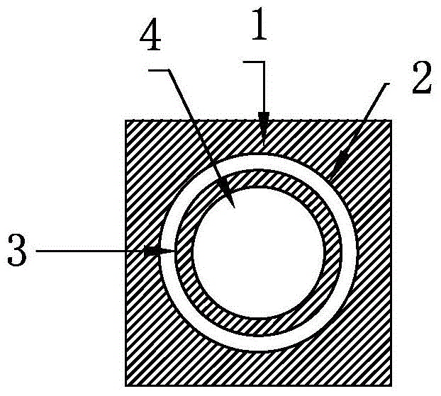
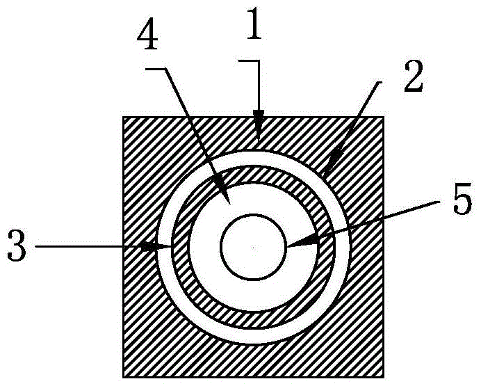
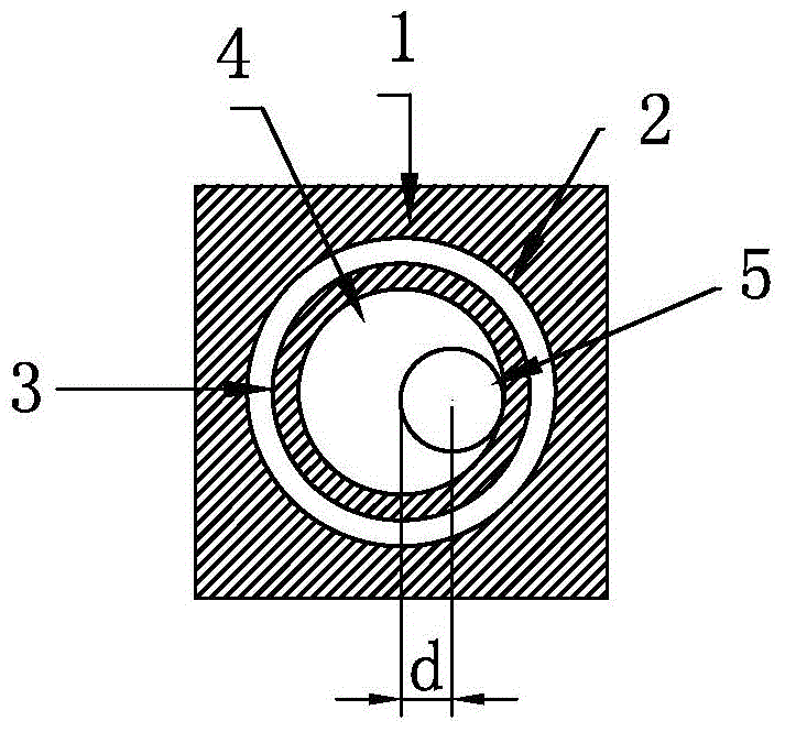
The invention discloses a multi-layer circuit board with the high mechanical hole drilling yield and a manufacturing method of the multi-layer circuit board. The multi-layer circuit board can improve the circuit via hole drilling yield, is convenient to operate and saves time and labor. At least three identification rings are evenly arranged in the process waste areas of the four corners of a prearranged flexible printed circuit board of a multi-layer circuit board body before expansion and contraction in a staggered mode, the identification rings correspond to the circle centers at the of identification holes, to be drilled, marked at the identical positions of a design drilling band of circuit via holes to be drilled before expansion and contraction, each identification ring is composed of an outer ring body, a middle ring body and an inner circle, the outer ring body, the middle ring body and the inner circle of each identification riing share the same circle center, the outer rings and the inner circles are light transmitting areas, the middle rings are lighttight solid copper areas, retreating windows are arranged at the positions, corresponding to the identification rings, of other hard boards or flexible printed circuit boards overlapped on the upper portion and the lower portion of the prearranged flexible printed circuit board, and the identification rings can be observed through the retreating windows. The circuit via hole drilling yield can be greatly improved, the eccentric distance is fast detected through a visual method, and therefore the production efficiency of the multi-layer circuit board is greatly improved.

Description

technical field [0001] The invention relates to a soft and hard multi-layer circuit board, in particular to a soft and hard multi-layer circuit board that can still improve the yield rate of mechanically drilled circuit via holes of the multi-layer circuit board when the multi-layer circuit board has expansion and contraction deviation after lamination. Rigid multilayer circuit board and its manufacturing method. Background technique [0002] Ordinary circuit boards are divided into single-sided wiring and double-sided wiring, commonly known as single-sided and double-sided. However, due to the limited design space of high-end electronic products, in addition to surface wiring, multi-layer circuits have to be superimposed inside. In the production process, after making each layer of circuit, through positioning, pressing and other processes, the multi-layer circuit is superimposed through the bonding sheet to form a multi-layer circuit board. Generally, circuit boards with ...

Claims


Application Information

Patent Timeline
Patent Type & Authority Patents(China)
IPC IPC(8): H05K1/02H05K3/00H05K3/46H05K3/42
Inventor 潘陈华孙建光郭瑞明何清华曹焕威
Owner SHENZHEN HUALIN CIRCUIT TECH
Learn More