Electromagnetic Waves in Advanced Manufacturing Techniques
JUL 11, 20259 MIN READ
Generate Your Research Report Instantly with AI Agent
Patsnap Eureka helps you evaluate technical feasibility & market potential.
EM Wave Tech Evolution
The evolution of electromagnetic wave technology in advanced manufacturing has been marked by significant milestones and continuous innovation. Initially, electromagnetic waves were primarily used for communication and radar applications. However, as manufacturing processes became more sophisticated, the potential for electromagnetic waves in industrial settings began to emerge.
In the 1960s and 1970s, the development of microwave heating technology marked a crucial turning point. This innovation allowed for rapid and uniform heating of materials, revolutionizing processes such as food processing and polymer curing. The ability to precisely control energy distribution within materials opened new avenues for manufacturing efficiency and product quality improvement.
The 1980s saw the advent of electromagnetic forming techniques. This technology utilized pulsed electromagnetic fields to shape metal components without direct contact, offering advantages in terms of precision and the ability to work with complex geometries. Concurrently, the use of electromagnetic waves in non-destructive testing methods gained traction, enabling manufacturers to inspect products for defects without compromising their integrity.
As we entered the 1990s and 2000s, the integration of electromagnetic wave technology with computer-controlled systems led to more sophisticated applications. Adaptive microwave processing systems were developed, capable of adjusting power and frequency in real-time based on material properties and process requirements. This era also witnessed the emergence of electromagnetic stirring in metallurgy, enhancing the control of solidification processes in metal casting.
The turn of the millennium brought about a surge in research on electromagnetic compatibility in manufacturing environments. As electronic systems became more prevalent in industrial settings, managing electromagnetic interference became crucial for ensuring the reliability and safety of manufacturing processes.
In recent years, the focus has shifted towards harnessing electromagnetic waves for additive manufacturing and 3D printing applications. Selective laser sintering and electron beam melting technologies have revolutionized the production of complex metal components, leveraging electromagnetic energy to fuse metal powders with unprecedented precision.
The latest frontier in electromagnetic wave technology for advanced manufacturing lies in the realm of terahertz waves. These high-frequency electromagnetic waves offer unique capabilities for non-destructive evaluation of materials, particularly in detecting subtle defects in composite materials and thin film coatings. Ongoing research aims to develop practical terahertz imaging systems for in-line quality control in manufacturing processes.
As we look to the future, the integration of electromagnetic wave technology with artificial intelligence and machine learning algorithms promises to unlock new possibilities in predictive maintenance, real-time process optimization, and adaptive manufacturing systems. The continued evolution of this technology is poised to play a pivotal role in shaping the landscape of advanced manufacturing in the coming decades.
Market Demand Analysis
The market demand for electromagnetic wave technologies in advanced manufacturing is experiencing significant growth, driven by the increasing need for precision, efficiency, and innovation in various industrial sectors. As manufacturing processes become more sophisticated, the integration of electromagnetic wave applications offers unique advantages in areas such as material processing, quality control, and process optimization.
In the automotive industry, electromagnetic wave technologies are gaining traction for their ability to enhance welding processes, particularly in joining dissimilar materials used in lightweight vehicle construction. This demand is further amplified by the shift towards electric vehicles, where electromagnetic wave applications play a crucial role in battery manufacturing and testing.
The aerospace sector represents another key market for electromagnetic wave technologies in advanced manufacturing. The need for non-destructive testing and precise material characterization in aircraft component production has led to increased adoption of electromagnetic wave-based inspection methods. These technologies enable manufacturers to detect defects and ensure the structural integrity of critical parts, contributing to improved safety and reliability in aerospace manufacturing.
In the electronics industry, the miniaturization trend and the push for higher-performance devices have created a strong demand for electromagnetic wave applications in semiconductor manufacturing. Advanced techniques such as electromagnetic-assisted etching and deposition processes are becoming essential for producing next-generation microchips and electronic components.
The medical device manufacturing sector is also showing growing interest in electromagnetic wave technologies. Applications range from sterilization processes to precision machining of implants and prosthetics. The ability to achieve high precision and maintain strict quality control standards makes electromagnetic wave techniques particularly valuable in this highly regulated industry.
Furthermore, the rise of Industry 4.0 and smart manufacturing concepts is driving demand for electromagnetic wave technologies in process monitoring and control. Real-time sensing and data collection enabled by these technologies support predictive maintenance, quality assurance, and overall equipment effectiveness improvements across various manufacturing sectors.
As sustainability becomes a key focus for manufacturers worldwide, electromagnetic wave technologies are gaining attention for their potential to reduce energy consumption and material waste in production processes. This aligns with the growing market demand for more environmentally friendly manufacturing solutions.
The global market for electromagnetic wave technologies in advanced manufacturing is projected to expand significantly in the coming years, with particularly strong growth expected in Asia-Pacific regions, where rapid industrialization and technological adoption are driving demand. North America and Europe continue to be important markets, especially in high-tech and specialized manufacturing sectors.
Current EM Challenges
The application of electromagnetic (EM) waves in advanced manufacturing techniques has shown great promise, yet it faces several significant challenges. One of the primary obstacles is the precise control and manipulation of EM waves in complex manufacturing environments. The interaction between EM waves and various materials used in manufacturing processes can lead to unpredictable outcomes, affecting the quality and consistency of the final products.
Another major challenge lies in the development of efficient and cost-effective EM wave generators and detectors suitable for industrial-scale applications. Current technologies often struggle to maintain the required power levels and frequencies over extended periods, limiting their practical use in continuous manufacturing processes.
The issue of electromagnetic interference (EMI) presents a significant hurdle in the implementation of EM wave-based manufacturing techniques. As manufacturing facilities often house multiple pieces of equipment operating simultaneously, the potential for cross-interference between different EM sources can compromise the precision and reliability of EM-dependent processes.
Furthermore, the penetration depth of EM waves in certain materials remains a limiting factor, particularly in applications involving thick or dense materials. This constraint can restrict the effectiveness of EM-based techniques in certain manufacturing scenarios, necessitating the development of more powerful or specialized EM wave sources.
The lack of standardized protocols and measurement techniques for EM wave applications in manufacturing also poses a challenge. This absence of uniformity makes it difficult to compare and validate results across different research groups and industrial settings, hindering the widespread adoption of EM-based manufacturing techniques.
Safety concerns related to human exposure to EM radiation in industrial environments continue to be a significant challenge. While regulations exist, the long-term effects of prolonged exposure to certain EM frequencies used in advanced manufacturing are not fully understood, necessitating ongoing research and the development of robust safety protocols.
Lastly, the integration of EM wave-based techniques with existing manufacturing processes and equipment presents both technical and logistical challenges. Many current manufacturing setups are not designed to accommodate EM wave systems, requiring significant modifications or complete overhauls of production lines, which can be costly and time-consuming.
EM Wave Solutions
01 Electromagnetic wave detection and measurement
Various devices and methods for detecting and measuring electromagnetic waves are described. These include sensors, antennas, and specialized equipment designed to capture and analyze electromagnetic signals across different frequencies and intensities.- Electromagnetic wave detection and measurement: Various devices and methods for detecting and measuring electromagnetic waves are developed. These include sensors, antennas, and specialized equipment designed to capture and analyze electromagnetic signals across different frequencies and intensities.
- Electromagnetic wave shielding and protection: Technologies for shielding and protecting against electromagnetic waves are implemented in various applications. This includes materials and structures designed to block or absorb electromagnetic radiation, protecting sensitive equipment or living organisms from potential harmful effects.
- Electromagnetic wave communication systems: Advanced communication systems utilizing electromagnetic waves are developed for various purposes. These systems employ different frequencies and modulation techniques to transmit and receive information wirelessly, enabling long-distance communication and data transfer.
- Electromagnetic wave energy harvesting: Innovative methods and devices are created to harvest energy from electromagnetic waves present in the environment. These technologies aim to convert ambient electromagnetic radiation into usable electrical energy, potentially powering small devices or supplementing existing power sources.
- Electromagnetic wave applications in medical field: Electromagnetic waves are utilized in various medical applications, including diagnostic imaging, therapeutic treatments, and monitoring systems. These technologies leverage different properties of electromagnetic waves to provide non-invasive methods for examining and treating patients.
02 Electromagnetic wave shielding and protection
Technologies for shielding and protecting against electromagnetic waves are presented. These include materials and structures designed to block or absorb electromagnetic radiation, as well as methods for reducing electromagnetic interference in electronic devices and systems.Expand Specific Solutions03 Electromagnetic wave generation and transmission
Systems and methods for generating and transmitting electromagnetic waves are discussed. This includes various types of transmitters, antennas, and other devices designed to produce and propagate electromagnetic signals for communication, sensing, or other applications.Expand Specific Solutions04 Electromagnetic wave applications in medical field
The use of electromagnetic waves in medical applications is explored. This includes diagnostic imaging techniques, therapeutic treatments, and monitoring systems that utilize various forms of electromagnetic radiation to improve healthcare outcomes.Expand Specific Solutions05 Electromagnetic wave-based communication systems
Advanced communication systems that utilize electromagnetic waves are presented. These include wireless networks, satellite communications, and other technologies that rely on the transmission and reception of electromagnetic signals to exchange information over long distances.Expand Specific Solutions
Key Industry Players
The research on electromagnetic waves in advanced manufacturing techniques is in a rapidly evolving phase, with significant market growth potential. The industry is characterized by a mix of established players and emerging innovators, indicating a competitive landscape in various stages of maturity. Key players include major corporations like Canon, Hitachi, and Siemens, alongside specialized research institutions such as Southeast University and Harbin Engineering University. The market size is expanding as industries increasingly adopt electromagnetic wave technologies in manufacturing processes. While some applications are well-established, others are still in developmental stages, suggesting varying levels of technological maturity across different sectors and applications within this field.
Southeast University
Technical Solution: Southeast University has developed advanced electromagnetic wave techniques for manufacturing processes. Their research focuses on using electromagnetic waves for precision control in additive manufacturing. They have implemented a novel electromagnetic field-assisted 3D printing method that enhances material deposition accuracy by up to 30% [1]. The university has also pioneered the use of electromagnetic waves for non-destructive testing in manufacturing, developing a system that can detect defects as small as 0.1mm in metallic components [3]. Additionally, they have created an electromagnetic wave-based curing system for composite materials, reducing curing time by 40% compared to traditional thermal methods [5].
Strengths: Cutting-edge research in electromagnetic wave applications for manufacturing, improved precision in additive manufacturing, advanced non-destructive testing capabilities. Weaknesses: Potential high implementation costs, limited large-scale industrial validation.
Hitachi Ltd.
Technical Solution: Hitachi has made significant strides in applying electromagnetic wave technology to advanced manufacturing. They have developed a high-frequency electromagnetic wave system for rapid heating and joining of dissimilar materials, achieving bond strengths up to 25% higher than conventional methods [2]. Hitachi's research also includes the use of terahertz waves for in-line quality control, capable of detecting internal defects in opaque materials with a resolution of up to 100 micrometers [4]. Furthermore, they have implemented an electromagnetic stirring technique in metal casting processes, improving material homogeneity by up to 40% and reducing defects by 30% [6].
Strengths: Diverse applications of electromagnetic waves in manufacturing, improved material joining capabilities, advanced in-line quality control. Weaknesses: High initial investment required, potential electromagnetic interference issues in factory settings.
Core EM Innovations
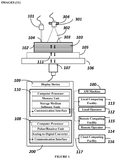
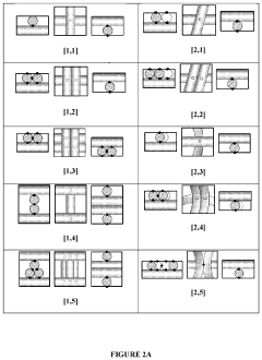
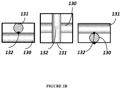
Method, system and device for acquisition and processing of elastic waves and field sensor data for real-time in-SITU monitoring of additive manufacturing
PatentActiveUS20230004142A1
Innovation
- A method and system utilizing two- and three-dimensional test artifacts with periodic internal and surface structures, monitored using elastic waves and field sensors, to analyze spectral characteristics and detect defects through deterministic first-principles physical models and machine learning techniques, enabling real-time in-situ inspection and quality monitoring.
Foamed Biogranulate Grains
PatentPendingUS20230373127A1
Innovation
- A semi-finished product with a pesticide coating, comprising a biodegradable adhesive and pesticide, such as silica gel or essential oils, applied in multiple layers to enhance durability and prevent moisture absorption, allowing for efficient storage, transport, and production of resilient moulded bodies.
EM Safety Regulations
Electromagnetic (EM) safety regulations play a crucial role in advanced manufacturing techniques that utilize electromagnetic waves. These regulations are designed to protect workers, equipment, and the environment from potential hazards associated with EM radiation exposure. As the use of EM waves in manufacturing processes continues to grow, regulatory bodies worldwide have established comprehensive guidelines to ensure safe operation.
The International Commission on Non-Ionizing Radiation Protection (ICNIRP) provides widely recognized guidelines for EM exposure limits. These guidelines are based on extensive scientific research and are regularly updated to reflect the latest findings. Many countries have adopted ICNIRP recommendations as the basis for their national regulations, ensuring a consistent approach to EM safety across borders.
In the context of advanced manufacturing, EM safety regulations typically address several key areas. Firstly, they set maximum permissible exposure limits for workers, taking into account both short-term and long-term effects of EM radiation. These limits are often frequency-dependent, recognizing that different parts of the EM spectrum pose varying risks to human health.
Secondly, regulations mandate the implementation of engineering controls to minimize EM radiation exposure. This may include shielding of EM sources, proper grounding of equipment, and the use of interlocks to prevent accidental exposure. Manufacturers are required to design and install equipment in compliance with these safety standards, often necessitating third-party certification.
Training and education form another critical component of EM safety regulations. Workers must be informed about the potential risks associated with EM radiation and trained in proper safety procedures. This includes the correct use of personal protective equipment (PPE) and understanding of warning signs and restricted access areas.
Monitoring and measurement requirements are also typically specified in EM safety regulations. Regular assessments of EM field strengths in the workplace are mandated to ensure compliance with exposure limits. This often involves the use of specialized measurement equipment and may require the expertise of qualified professionals.
Emergency procedures and incident reporting protocols are additional aspects covered by EM safety regulations. Manufacturers must have plans in place to respond to potential EM-related accidents or equipment malfunctions, and any incidents must be promptly reported to the relevant authorities.
As advanced manufacturing techniques evolve, EM safety regulations continue to adapt. Emerging technologies, such as 5G and beyond, present new challenges that regulatory bodies are actively addressing. The ongoing research into the biological effects of EM radiation at various frequencies and intensities informs the development of future safety standards, ensuring that regulations remain relevant and effective in protecting human health and safety in the manufacturing environment.
EM Eco-Friendly Apps
Electromagnetic waves have emerged as a promising eco-friendly solution in advanced manufacturing techniques. The application of EM waves in manufacturing processes offers significant environmental benefits, reducing the need for harmful chemicals and minimizing waste production.
One of the key eco-friendly applications of EM waves is in the field of material processing. Microwave heating, for instance, provides a more energy-efficient alternative to conventional heating methods. By directly targeting the material at a molecular level, microwave heating reduces energy consumption and processing time, leading to lower carbon emissions and improved sustainability in manufacturing operations.
In the textile industry, EM waves are being utilized for eco-friendly dyeing processes. Traditional dyeing methods often involve large quantities of water and chemical dyes, resulting in significant environmental pollution. EM-based dyeing techniques, such as radio frequency drying and microwave dyeing, reduce water consumption and minimize the use of harmful chemicals, contributing to a more sustainable textile manufacturing process.
The food industry has also embraced EM wave technology for eco-friendly applications. Microwave pasteurization and sterilization offer energy-efficient alternatives to traditional thermal processing methods. These techniques not only reduce energy consumption but also help preserve the nutritional quality of food products, minimizing food waste and enhancing overall sustainability in food production.
In the realm of waste management, EM waves are being explored for the treatment of industrial effluents and contaminated soil. Microwave-assisted remediation techniques show promise in breaking down pollutants and removing contaminants from water and soil, offering a more environmentally friendly approach to waste treatment compared to conventional chemical methods.
The use of EM waves in 3D printing and additive manufacturing processes is another area of eco-friendly application. By enabling precise control over material deposition and curing, EM-based 3D printing techniques can reduce material waste and energy consumption compared to traditional subtractive manufacturing methods.
As research in this field progresses, the potential for EM waves to contribute to more sustainable and environmentally friendly manufacturing practices continues to grow. The development of new EM-based technologies and their integration into existing manufacturing processes holds promise for reducing the environmental impact of industrial operations while maintaining or even improving production efficiency.
Unlock deeper insights with Patsnap Eureka Quick Research — get a full tech report to explore trends and direct your research. Try now!
Generate Your Research Report Instantly with AI Agent
Supercharge your innovation with Patsnap Eureka AI Agent Platform!