
Bonding pad structure for back illuminated optoelectronic device and fabricating method thereof

a technology of optoelectronic devices and bonding pads, which is applied in the direction of semiconductor devices, line/current collector details, semiconductor/solid-state device details, etc., can solve the problems of reducing package reliability, poor adhesion between bonding wires and bonding pads, and atoms of barrier layers leaking into

Active Publication Date: 2010-03-16
VISERA TECH CO LTD
View PDF4 Cites 5 Cited by
  • Summary
  • Abstract
  • Description
  • Claims
  • Application Information

AI Technical Summary

Benefits of technology

The patent text describes a bonding pad structure for optoelectronic devices and methods for fabricating it. The structure includes a carrier substrate with a bonding pad region and an optoelectronic device region, an insulating layer with an opening corresponding to the bonding pad region, at least one bonding pad embedded in the insulating layer, a device substrate, a cap layer, and a conductive buffer layer. The optoelectronic device can be a device substrate or a metal pad with no barrier layers. The method involves removing the device substrate and forming a cap layer on the insulating layer. The insulating layer is then etched to expose the bonding pad, and a conductive buffer layer is formed in the opening to directly contact the bonding pad. The technical effects of the patent text include improved bonding pad reliability and stability, simplified fabrication processes, and improved device performance.

Problems solved by technology

However, the atoms of the barrier layer may diffuse into the bottom surfaces and sidewalls of the metal structures during performing thermal process in device fabrication.
However, as the device substrate is reversely arranged on the carrier substrate and partially removed to expose the bonding pads, the bonding wire may contact the surface of the bonding pad with impurities diffusing from the barrier layer, resulting in poor adhesion between the bonding wires and the bonding pads.
Poor adhesion between the bonding wire and the bonding pad may reduce package reliability and cause device failure.

Method used


Image

  • Bonding pad structure for back illuminated optoelectronic device and fabricating method thereof
  • Bonding pad structure for back illuminated optoelectronic device and fabricating method thereof
  • Bonding pad structure for back illuminated optoelectronic device and fabricating method thereof

Examples


Embodiment Construction

[0016]The following description is of the best-contemplated mode of carrying out the invention. This description is provided for the purpose of illustrating the general principles of the invention and should not be taken in a limiting sense. The scope of the invention is best determined by reference to the appended claims.

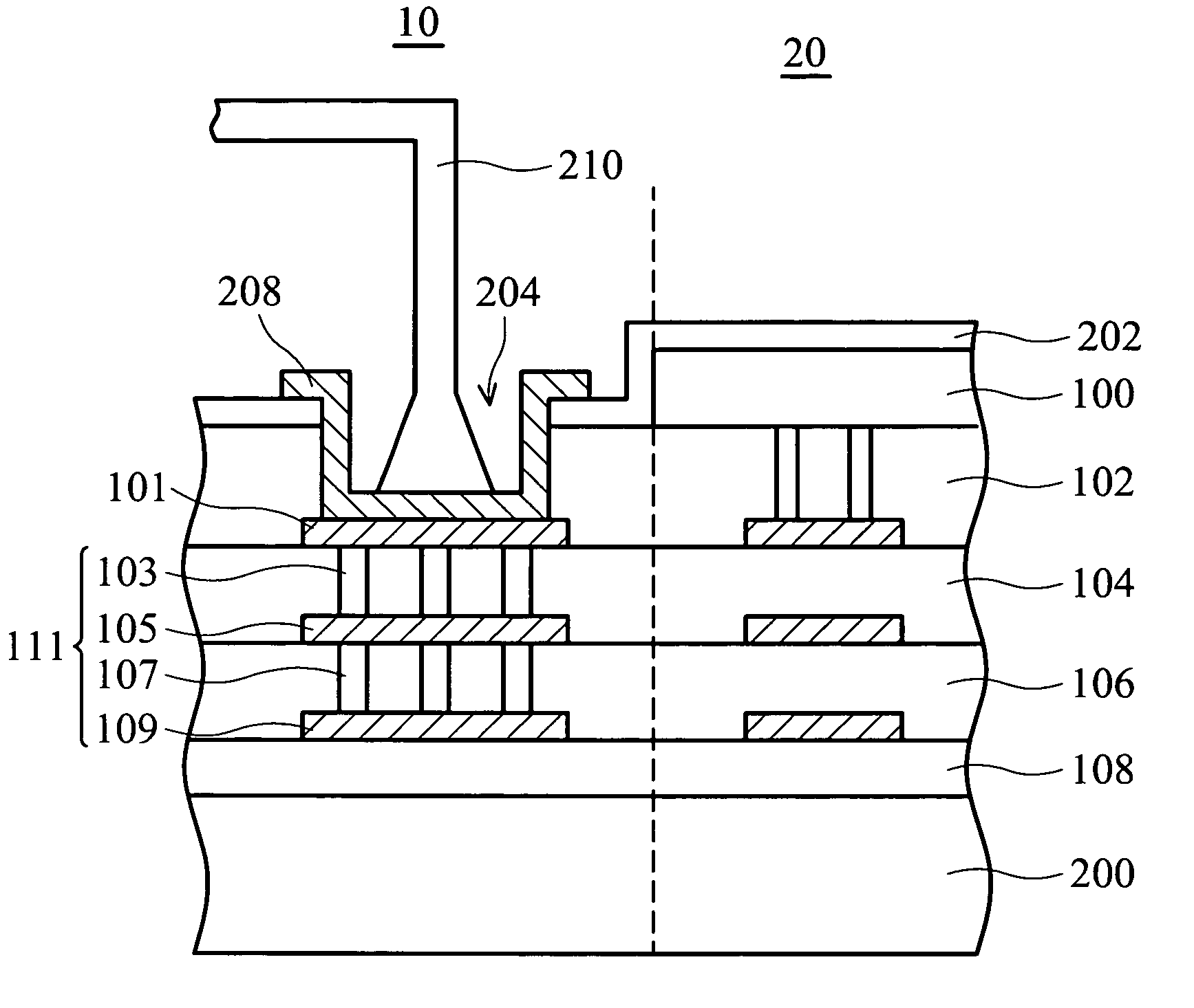
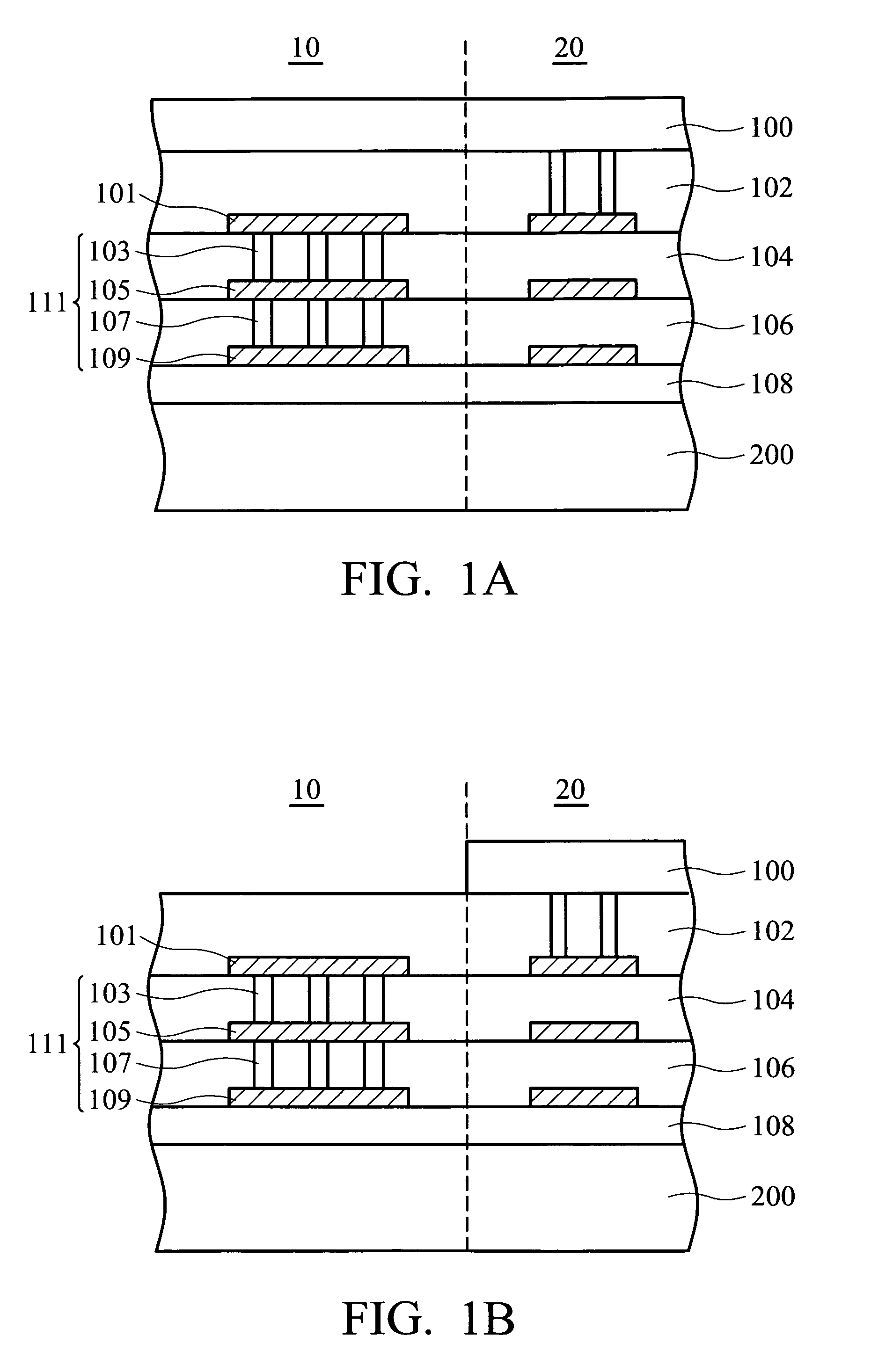
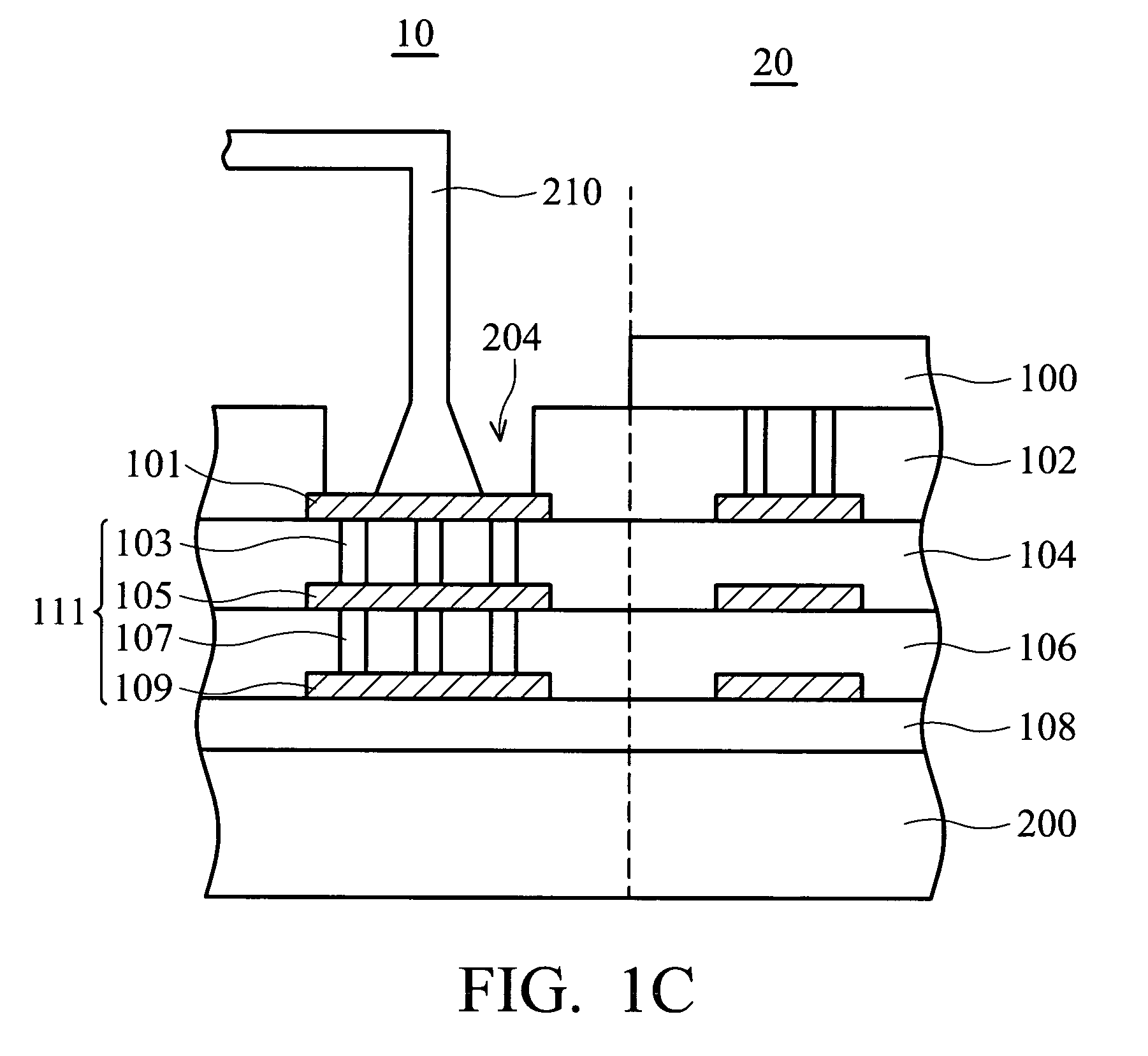
[0017]The invention relates to a bonding pad structure for an optoelectronic device and a method for fabricating the same. FIG. 1C illustrates an embodiment of a bonding pad structure for an optoelectronic device, such as a back-illuminated image sensor. The bonding pad structure comprises a carrier substrate 200, such as a silicon substrate, having a bonding pad region 10 and an optoelectronic device region 20. An insulating layer is disposed on the carrier substrate 200, having an opening 204 corresponding to the bonding pad region 10. In this embodiment, the insulating layer comprises dielectric layers 108, 106, 104 and 102 successively disposed on the carrier s...


PUM

PropertyMeasurementUnit
conductiveaaaaaaaaaa
structureaaaaaaaaaa
adhesionaaaaaaaaaa

Abstract

A bonding pad structure for an optoelectronic device. The bonding pad structure comprises a carrier substrate having a bonding pad region and an optoelectronic device region. An insulating layer is disposed on the carrier substrate, having an opening corresponding to the bonding pad region. A bonding pad is embedded in the insulating layer under the opening to expose the top surface thereof. A device substrate is disposed on the insulating layer corresponding to the optoelectronic device region. A cap layer covers the device substrate and the insulating layer excluding the opening. A conductive buffer layer is disposed in the opening to directly contact the bonding pad. The invention also discloses a method for fabricating the same.

Description

BACKGROUND OF THE INVENTION[0001]1. Field of the Invention[0002]The invention relates to optoelectronic devices and in particular to a bonding pad structure for an optoelectronic device and fabricating method thereof.[0003]2. Description of the Related Art[0004]Digital image devices are widely used in, for example, digital cameras, digital video recorders, cellular phones with image capture function, and monitors. A digital imaging sensor typically includes an optoelectronic device chip, such as a charge-coupled device (CCD) image sensor chip and CMOS image sensor chip.[0005]Such an image sensor chip typically comprises metal structures used as electrodes for picture elements and as bonding pads for electrical connection with external circuits. The metal structure is formed by known damascene process and metallization. A barrier layer is typically formed prior to metal filling. That is, the barrier layer is formed on the bottom surfaces and sidewalls of the metal structures. However...

Claims


Application Information

Patent Timeline
Patent Type & Authority Patents(United States)
IPC IPC(8): H01L23/48H01L23/52H01L29/40
CPCH01L24/03H01L24/48H01L24/05Y10T29/49224H01L2224/04042H01L2224/05073H01L2224/05093H01L2224/05096H01L2224/05567H01L2224/05572H01L2224/05624H01L2224/05639H01L2224/05644H01L2224/05647H01L2224/48463H01L2224/85375H01L2924/01006H01L2924/01013H01L2924/01014H01L2924/01027H01L2924/01029H01L2924/01047H01L2924/01078H01L2924/01079H01L2924/19043H01L2924/0002H01L2224/05556H01L2224/8585H01L2924/01033H01L2924/01019H01L2924/00014H01L2224/05552H01L2224/45099
Inventor WANG, KAI-CHIHLIU, FANG-CHANG
Owner VISERA TECH CO LTD
Learn More