
Capacitive touch sensor, manufacturing method therefor, and display device

a technology of capacitive touch and manufacturing method, which is applied in the direction of instruments, other domestic objects, chemistry apparatus and processes, etc., can solve the problems of recent attention to capacitive touch panels, suppress the pattern visibility caused by step formation, and prevent further suppressing or preventing pattern formation

Active Publication Date: 2015-10-01
NISSHA PRINTING COMPANY
View PDF0 Cites 10 Cited by
  • Summary
  • Abstract
  • Description
  • Claims
  • Application Information

AI Technical Summary

Benefits of technology

The present invention is a capacitive touch sensor that has a unique structure and method of manufacturing. The sensor has first and second layers of conductive portions that intersect each other and are insulated from each other by intermediate insulating portions. The insulating portions are formed between the first and second layers, and between the second and first layers, respectively. This structure reduces steps between the conductive portions and improves pattern visibility, resulting in less visible or no visible pattern. The use of conductive polymers in the layers further improves pattern visibility. The manufacturing method of the sensor allows for easy and quick patterning of the layers.

Problems solved by technology

In contrast, touch panels of the capacitive type enable the detection of multiple points, what is called multi-touch, which cannot be achieved by those of the ordinary resistive film type, and therefore, capacitive touch panels have recently been attracting much attention.

Method used


Image

  • Capacitive touch sensor, manufacturing method therefor, and display device
  • Capacitive touch sensor, manufacturing method therefor, and display device
  • Capacitive touch sensor, manufacturing method therefor, and display device

Examples


examples

[0101]The present invention will hereinafter be described more specifically by way of Examples, but the present invention is not limited to the following Examples. The present invention can be put into practice after appropriate modifications or variations within a range meeting the gist described above and below, all of which are included in the technical scope of the present invention.

[0102]1. Evaluation of Pattern Visibility

[0103]The capacitive touch sensor 1 using PEDOT / PSS as the material of each of the first layer 10, the intermediate layer 12, and the second layer 15 was measured for haze and transmittance in Example 1. The term “haze” means a degree of cloudiness, and its lower values indicate higher brightness upon projecting. A conventional capacitive touch sensor as described below was used in Comparative Example 1.

[0104]FIG. 7A is a plan view showing the structure of the capacitive touch sensor according to Comparative Example 1. FIG. 7B is a cross-sectional view taken a...


PUM

PropertyMeasurementUnit
thicknessaaaaaaaaaa
light transmittanceaaaaaaaaaa
temperatureaaaaaaaaaa

Abstract

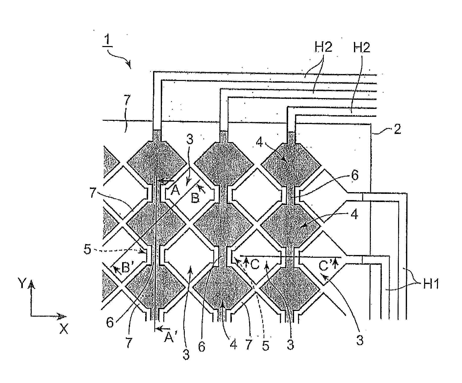
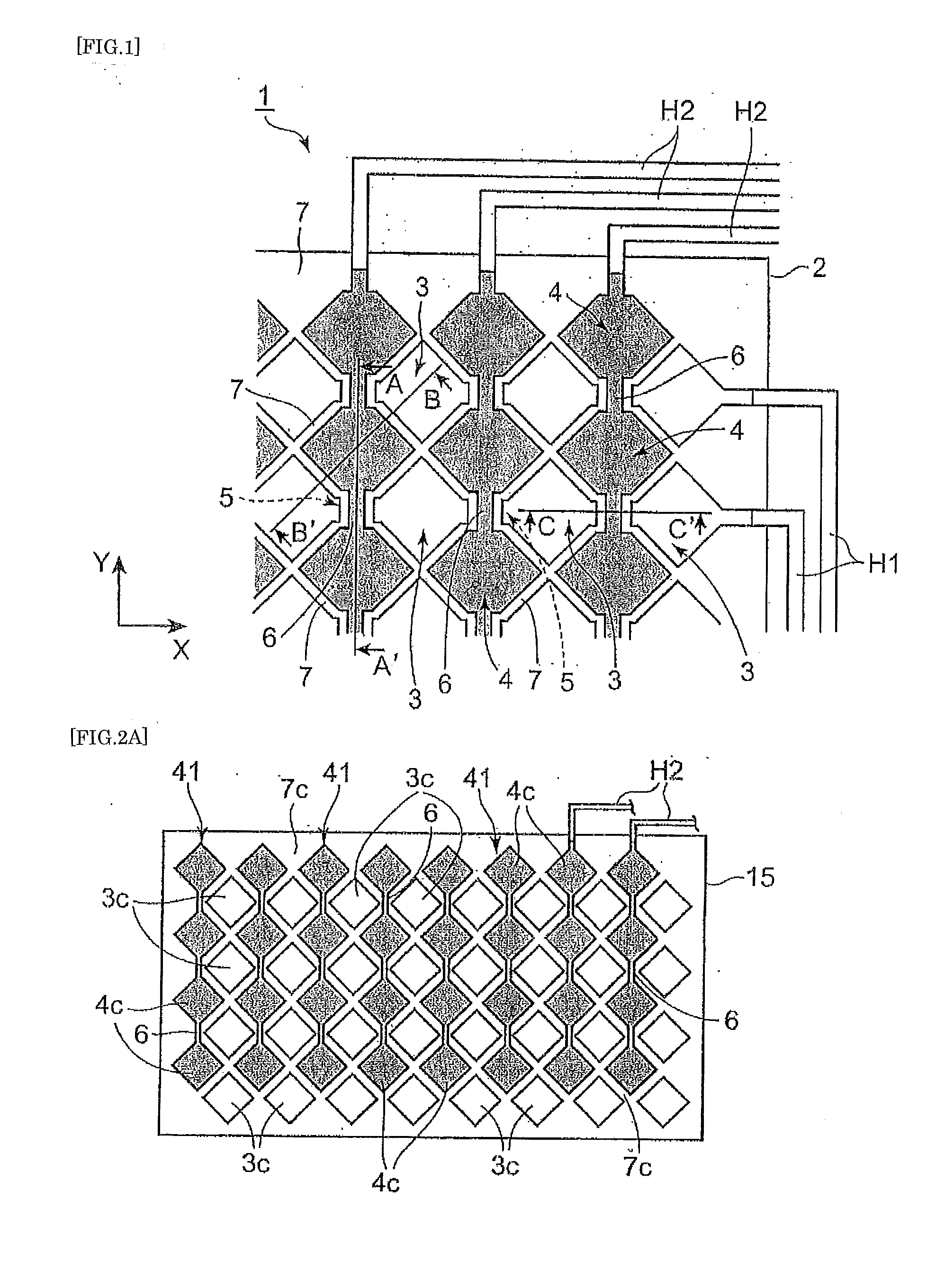
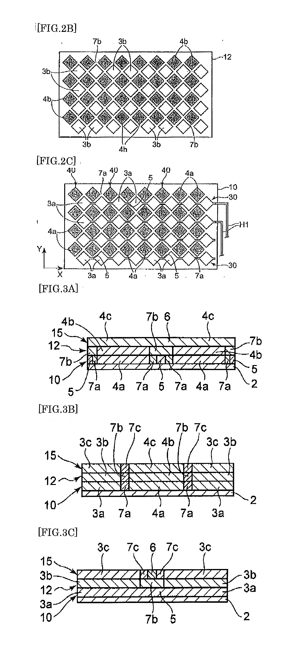
Provided herein are a capacitive touch sensor capable of reducing pattern visibility, a manufacturing method therefor, and a display device with the touch sensor. In a capacitive touch sensor (1), a first layer (10) has first first-layer electrodes (3a); first-layer conductive portions (5) connecting the adjacent first first-layer electrodes (3a); second first-layer electrodes (4a); and first-layer insulating portions (7a) formed between the second first-layer electrodes (4a) and the first-layer conductive portions (5). An intermediate layer (12) has first intermediate-layer electrodes (3b) formed on the first first-layer electrodes (3a); second intermediate-layer electrodes (4b) formed on the second first-layer electrodes (4a); and intermediate-layer insulating portions (7b) formed between the first-layer conductive portions (5) and second-layer conductive portions (6). A second layer (15) has first second-layer electrodes (3c); second second-layer electrodes (4c); second-layer conductive portions (6) connecting the adjacent second second-layer electrodes (4c) in the Y-axis direction so as to intersect with the first-layer conductive portions (5); and second-layer insulating portions (7c) formed between the first second-layer electrodes (3c) and the second-layer conductive portions (6).

Description

TECHNICAL FIELD[0001]The present invention relates to a capacitive touch sensor applicable to input devices each having a liquid crystal panel or another image screen, such as mobile phones, PDAs, and small PCs; a manufacturing method therefor; and a display device with the capacitive touch sensor.BACKGROUND ART[0002]In recent years, liquid crystal display devices (LCDs), organic light emitting devices (OLEDs), or others, have been used for various purposes. Even many displays to be used outdoors make use of LCDs.[0003]Further, LCDs have widely been used for dashboard panels, such as of vehicles, ships, or airplanes; car-mounted navigation systems; digital cameras; mobile devices such as mobile phones or personal computers; or digital signage to be used in, for example, buildings or supermarkets.[0004]In such electronic equipment, there have widely been used touch sensors, each serving as a display and an input means.[0005]Touch panels ordinarily used are of the optical type, ultras...

Claims


Application Information

Patent Timeline
Patent Type & Authority Applications(United States)
IPC IPC(8): G06F3/044
CPCG06F3/044G06F2203/04104G06F2203/04103B32B37/02B32B2309/105B32B2457/206B32B2457/208G06F2203/04111G06F3/0445G06F3/0446Y10T29/49105
Inventor NAKAMURA, KAZUTO
Owner NISSHA PRINTING COMPANY
Learn More