
High aspect ratio and reduced undercut trench etch process for a semiconductor substrate

a semiconductor substrate and trench etching technology, applied in the field of semiconductor processing methods, can solve the problems of etching profile control, sidewall scalloping and undercutting of etched structures, and the bosch process, as known in the art, to achieve the effect of improving the overall etch ra

Active Publication Date: 2013-05-02
ZEON CORP +1
View PDF4 Cites 38 Cited by
  • Summary
  • Abstract
  • Description
  • Claims
  • Application Information

AI Technical Summary

Benefits of technology

The patent describes a process for making semiconductor devices using a special gas called hydrofluorocarbon. This gas is used to make a protective layer on the sidewalls of a deep trench in the semiconductor substrate. This layer helps prevent the sidewalls from being damaged during the process of etching. As a result, the overall rate of etching can be increased while also protecting the substrate.

Problems solved by technology

However, the Bosch process, as known in the art, has several limitations.
One of such limitations is control of etch profile.
Specifically, the cyclical nature of the Bosch process results in sidewall scalloping and undercutting of the etched structures.
However, increasing the amount of the passivation gas supplied into the process chamber to reduce sidewall scalloping and undercutting significantly reduces the etch rate of the process, thereby severely limiting the throughput of the process.
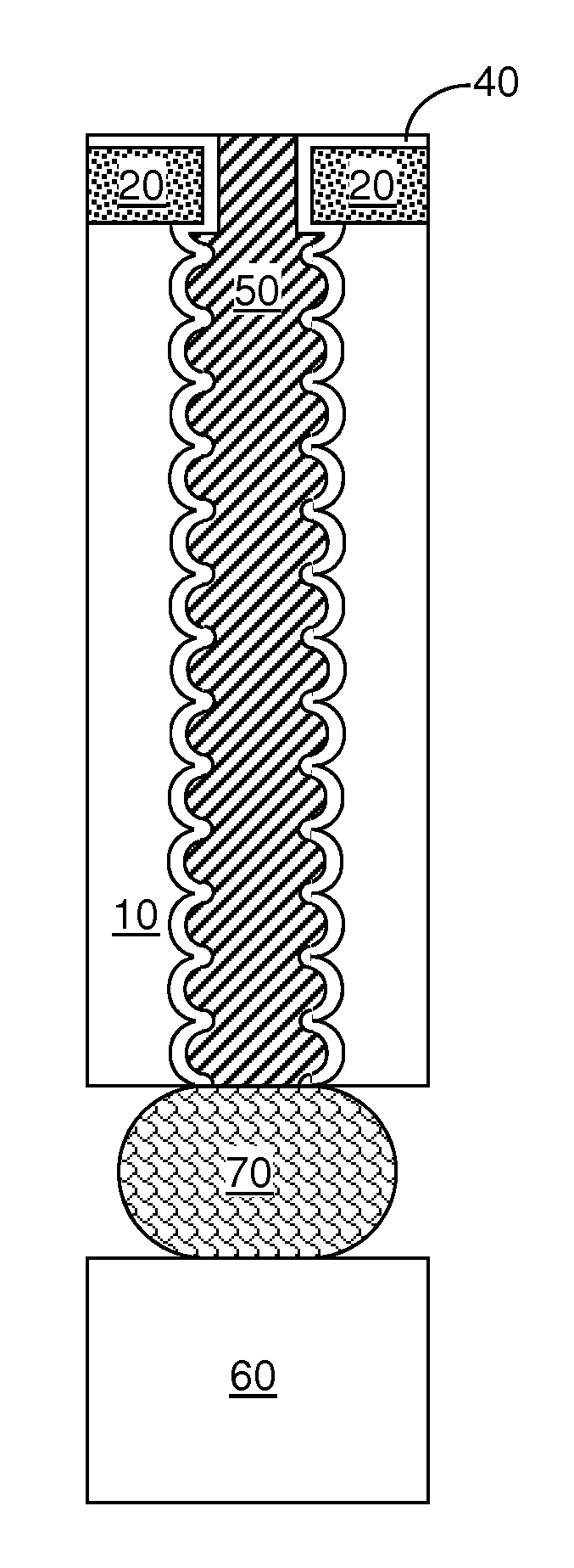
Undercutting of the hard mask results in formation of voids in a through substrate via that is subsequently formed by filling the trench with a conductive material.

Method used


Image

  • High aspect ratio and reduced undercut trench etch process for a semiconductor substrate
  • High aspect ratio and reduced undercut trench etch process for a semiconductor substrate
  • High aspect ratio and reduced undercut trench etch process for a semiconductor substrate

Examples


examples

[0063]Non-limiting examples of specific embodiments of the present disclosure are illustrated below, which demonstrate advantages of selected embodiments of the present disclosure. The non-limiting examples are for illustrative purposes only, and do not limit the scope of the present disclosure by any means.

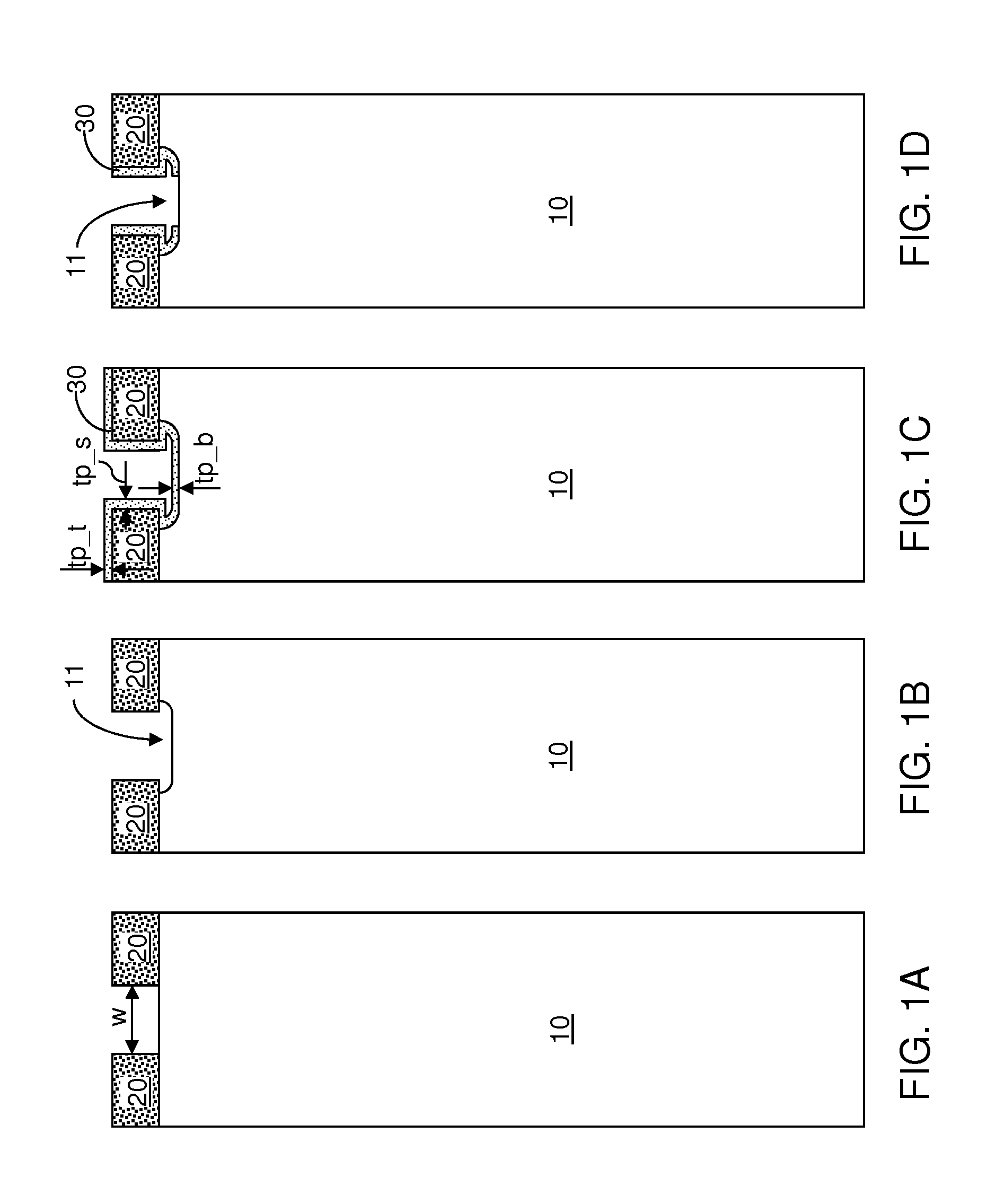
[0064]Referring to FIG. 4, the deposition rates of the hydrofluorocarbon polymer material at various portions of the hydrofluorocarbon polymer layer 30 is plotted for the case in which the fluorocarbon gas employed to generate the plasma during the deposition step is C5HF7 gas. In this example, the plasma pressure was 25 mTorr, the depth of the trench 11′ was 120 microns, and the width of the trench 11′ was 70 microns. The flow rate of the C5HF7 gas was 150 sccm, and the temperature of the process chamber was 20 degrees Celsius. In the graph, the horizontal axis indicates the RF power coupled to the plasma in Watts.

[0065]In the graph of FIG. 4, the deposition rates for the first ...


PUM


Abstract

A hydrofluorocarbon gas is employed as a polymer deposition gas in an anisotropic etch process employing an alternation of an etchant gas and the polymer deposition gas to etch a deep trench in a semiconductor substrate. The hydrofluorocarbon gas can generate a thick carbon-rich and hydrogen-containing polymer on sidewalls of a trench at a thickness on par with the thickness of the polymer on a top surface of the semiconductor substrate. The thick carbon-rich and hydrogen-containing polymer protects sidewalls of a trench, thereby minimizing an undercut below a hard mask without degradation of the overall rate. In some embodiments, an improvement in the overall etch rate can be achieved.

Description

BACKGROUND[0001]The present disclosure relates to semiconductor processing methods, and particularly to methods for anisotropically etching a high aspect ratio trench in a semiconductor substrate while minimizing an undercut, and structures for effecting the same.[0002]High aspect ratio deep silicon etch techniques are a key enabling technology for implementing through silicon via structures and three-dimensional integration of multiple semiconductor substrates. State of the art deep silicon etch utilizes a time modulated etch process, which is typically referred to as a “Bosch” process.[0003]The Bosch process employs alternating cycles of etching employing a SF6 gas and polymer deposition employing a passivation gas, which is a fluorocarbon gas that does not include hydrogen. The Bosch process provides a reasonable level of anisotropy required for forming high aspect ratio structures. However, the Bosch process, as known in the art, has several limitations. One of such limitations ...

Claims


Application Information

Patent Timeline
IPC IPC(8): H01L21/768H01L23/00
CPCH01L21/76898H01L29/0657H01L21/30655
Inventor FULLER, NICHOLAS C. M.JOSEPH, ERIC A.SIKORSKI, EDMUND M.MATSUURA, GOH
Owner ZEON CORP
Learn More