Wafer shape evaluating method and device producing method, wafer and wafer selecting method

Inactive Publication Date: 2003-01-30
RENESAS TECH CORP +1
View PDF6 Cites 41 Cited by
  • Summary
  • Abstract
  • Description
  • Claims
  • Application Information

AI Technical Summary

Benefits of technology

[0015] With the foregoing difficulties of the prior art in view, it is an object of the present invention to provide a method and an apparatus for evaluating a wafer configuration which, by evaluating quality of a wafer configuration from a different viewpoint from the conventional SFQR or the like, are capable of more precisely evaluating the peripheral portion of the wafer to manufacture a wafer suitable for each device fabricating process and improve production efficiency in the device fabricating process and the subsequent processes.
[0016] Another object of the present invention is to provide a device fabricating method, a wafer, and a wafer sorting method which, by evaluating quality of a wafer configuration from a different viewpoint from the conventional SFQR or the like using the above-mentioned evaluating method and apparatus, are capable of more precisely evaluating undulation on a wafer surface and the peripheral portion of a wafer to supply a wafer suitable for each device fabricating process, especially a process using an exposure system, and improve production efficiency in the device fabricating process and subsequent processes.
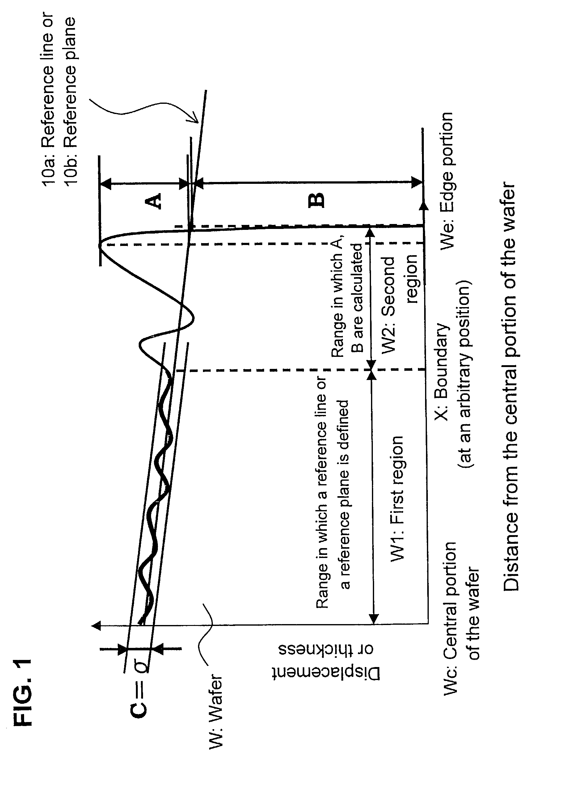
[0021] Here, the wafer configuration measured at a plurality of positions with a prescribed space within the wafer surface is displacement (height or roughness) in the direction vertical to the wafer surface or a wafer thickness. Evaluation on the displacement in the direction vertical to the wafer surface makes it possible to perform evaluation based on the front side reference. Further evaluation on the wafer thickness makes it possible to perform evaluation based on the back side reference.
[0033] Thus, the effect of rise in the peripheral portion of a wafer is great in the device fabricating process using an exposure system; it is preferable to make a value of the surface characteristic A (rise) obtained by the above-mentioned evaluating method as small as possible. Especially, it is effective to fabricate a device using an exposure system with a wafer of A=150 nm or less. It is preferable to make the rising components as small as possible, but it is not preferable to make sagging too large, so that the lower limit thereof is about -20 nm.
[0040] There could be conceivably various methods for meeting the above requirements: for instance, a first method in which a work is polished in a state that a coating film made of material having a polishing rate slower than that of a work is formed on the work peripheral portion to adjust a polishing rate thereon; a second method in which a work is polished in a manner that an improved means for holding a work is employed, that is the size of a work holding plate is improved, or a work is chucked at its peripheral portion by a work holding plate with a hard central portion of a work holding region and a soft peripheral portion thereof, and a third method in which a front surface of a work is polished in a manner that a back coating is formed on a back surface of a work and the work is held at the back coating, and in this method peripheral sags can also be controlled by differentiating the thickness of the back coating between the peripheral portion of the wafer and the central portion thereof to change the polishing pressure on the peripheral portion thereof.
[0045] Thus, by sorting wafers polished in the wafer manufacturing process, there can be obtained wafers more suitable for the device fabricating process, and the fabrication yield can further be improved.

Problems solved by technology

Recently, an integration level in a semiconductor device has been becoming increasingly higher because of the remarkable progress in the semiconductor device technology, and with this progress, a demand for quality of a silicon wafer or the like has also been becoming more severe.
With this progress, also a demand for quality of a silicon wafer or the like used as a base for a device has been becoming more severe.
That is, this is because a higher integration level of a semiconductor device has brought out miniaturization of a device size, and for instance, slight undulation or the like on a silicon wafer may lead to errors in a device pattern during the photolithography step or other steps.
As one of the important characteristics required to the silicon wafer as described above, there is a problem of shape quality thereof.
For instance, in the device fabricating process, many processing machines such as an exposure system and other machines are used, and compatibility between a wafer holding chuck used in each machine and a configuration of a wafer to be processed has been becoming an issue.
Matching between undulation and a peripheral shape of the chuck and those of the wafer is important, but it is impossible to evaluate the matching by the conventional indexes such as GBIR, SBIR, and SFQR.
Especially, there is a stepper (a popular name of a reduction projection step and repeat exposure system) wherein a wafer is stepped and exposed repeatedly to a projected figure through a mask pattern (a reticle patter); it was not necessarily possible to sort out wafers which are usable in the stepper in terms of configurations thererof by indexes such as SFQR.

Method used


Image

  • Wafer shape evaluating method and device producing method, wafer and wafer selecting method
  • Wafer shape evaluating method and device producing method, wafer and wafer selecting method
  • Wafer shape evaluating method and device producing method, wafer and wafer selecting method

Examples


first embodiment

[0073] Next, an evaluating apparatus for performing the above analysis is described below. FIG. 6 is a schematic explanatory view showing an essential structure of the apparatus for evaluating wafer configuration according to the present invention. An apparatus 20 for evaluating a wafer configuration shown in FIG. 6 is an apparatus used for measurement and analysis of displacement of a surface of a wafer W, which comprises a test stand 22, and a displacement measuring unit 26 having a displacement gauge 24 equipped with a laser oscillator or an automatic focusing mechanism, a computer 28, etc., and optically measures shifts in the distance from the previously calibrated reference point as the displacement. In the embodiment shown in FIG. 6, the displacement measuring unit 26 functions as a configuration measuring unit.

[0074] The test stand 22 is a stand used for placing thereon a silicon wafer W as an object to be measured. The displacement gauge 24 is an apparatus for irradiating a...

second embodiment

[0078] FIG. 7 is a schematic explanatory view showing an essential structure of the apparatus for evaluating a wafer configuration according to the present invention. In another embodiment for the apparatus for evaluating a wafer configuration, a thickness may be measured with a flatness measuring unit based on an electrostatic capacitance system in place of displacement of the wafer surface. The flatness measuring unit based on the electrostatic capacitance system is used as a thickness measurement unit 34 equipped with a thickness gauge 32 comprising electrostatic capacitance type of upper and lower sensors 32a, 32b arranged such that the wafer W is held between them as shown in FIG. 7, and measures the thickness of the wafer W by measuring the distances between the sensors 32a, 32b and upper and lower surfaces of the wafer W, respectively. As the flatness measuring unit based on the electrostatic capacitance system, a commercial non-contact type of wafer thickness, flatness and B...

##ventive example 1

Inventive Example 1

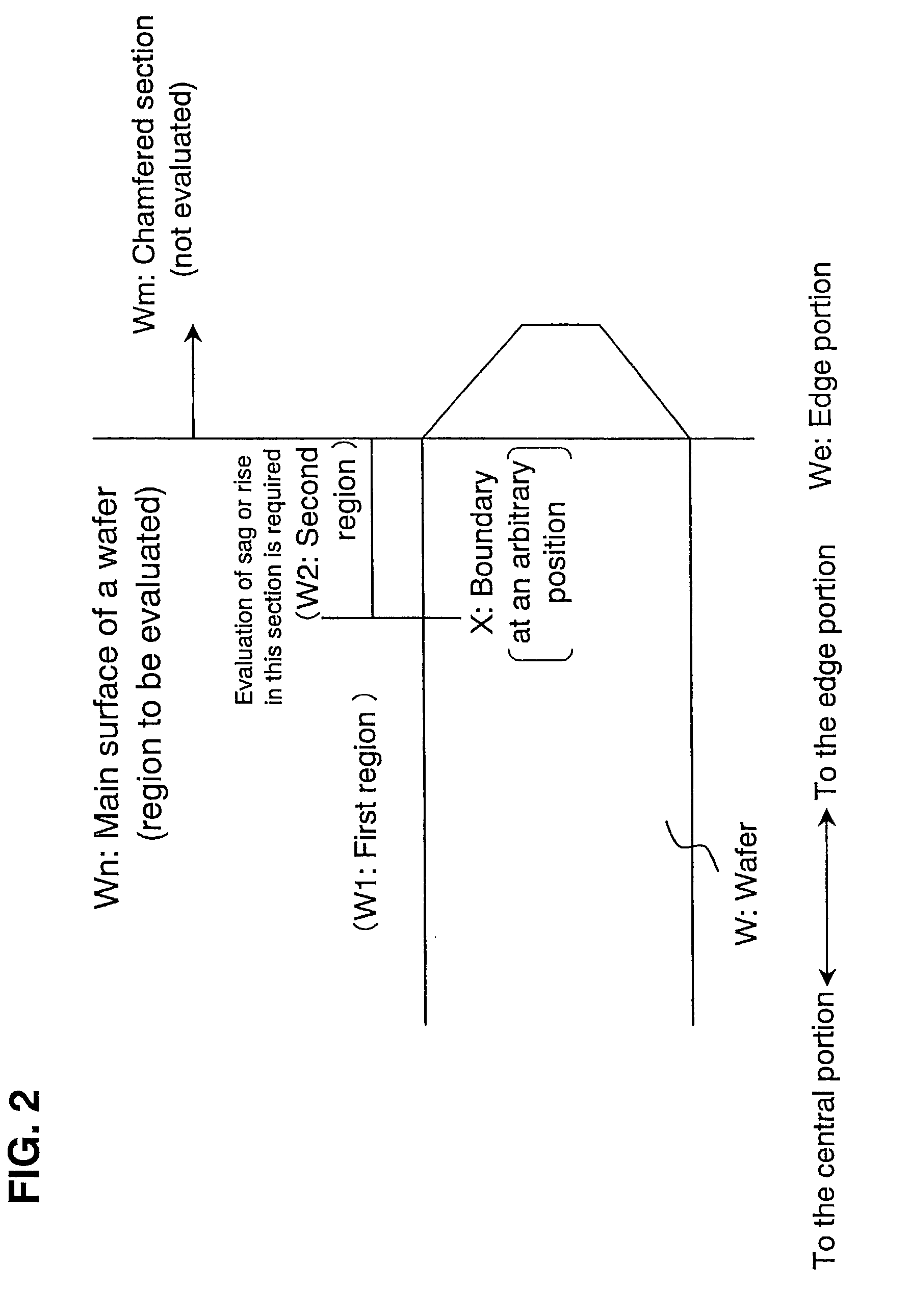
[0105] 8-inch mirror-polished wafers (200 mm in diameter and 0.5 mm in width of a peripheral edge portion being a chamfered portion) manufactured through various manufacturing processes (6 kinds) were evaluated by the evaluating method according to the present invention.

[0106] In the 6 kinds of wafer manufacturing processes (processes S1 to S6), different conditions were established in the etching step, surface grinding step and others. As for the yield in a device fabricating process, the above manufacturing processes are arranged in the order of S5>S6>S1>S4>S2>S3, and the process S5 was best, while a wafer manufactured in the process S3 was worst.

[0107] The evaluating method according to the present invention was used to evaluate what type of a wafer configuration is preferable for improving the yield in the device fabricating process. The analysis was performed through the method for evaluating a wafer configuration by preparing a reference line. There were ana...


PUM


Abstract

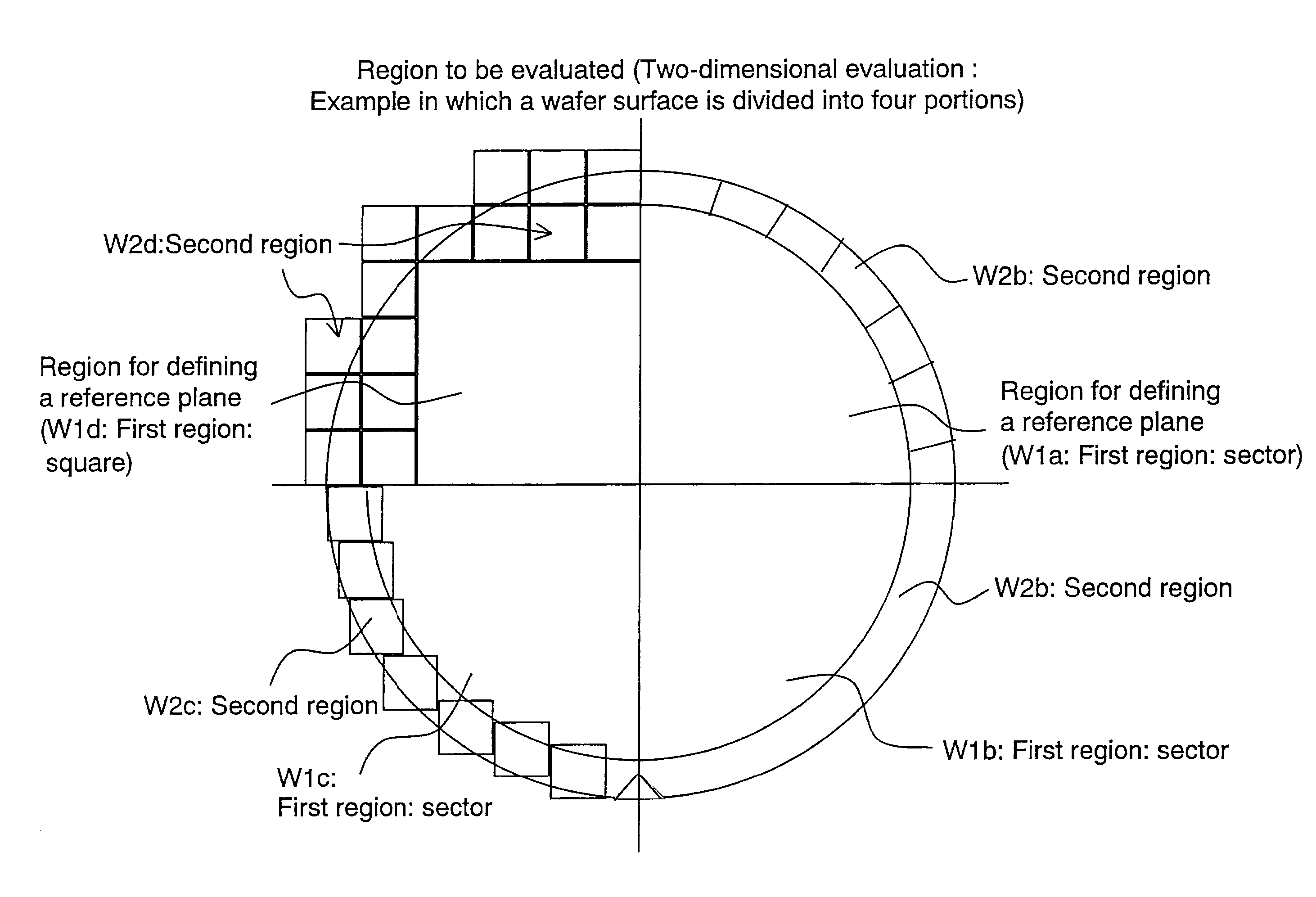
There are provided a method and an apparatus for evaluating a wafer configuration which can accurately evaluate a peripheral portion of a wafer as compared with the conventional SFQR or the like, which comprises: measuring a configuration of a wafer at positions with a prescribed space within a surface of the wafer; providing a first region (W1) within the wafer surface for calculating a reference line or a reference plane from the measured wafer configuration; calculating a reference line (10a) or a reference plane (10b) in the first region (W1); providing a second region (W2) to be evaluated outside the first region; extrapolating the reference line (10a) or reference plane (10b) to the second region (W2); analyzing a difference between the configuration of the second region and the reference line or reference plane within the second region; and calculating the analyzed difference as surface characteristics.

Description

TECHNICAL FIELD[0001] The present invention relates to a method and an apparatus for evaluating a configuration of a wafer represented by a silicon wafer. The present invention also relates to a semiconductor device fabricating method, especially to a wafer enabling improvement in a yield in a device fabricating process using an exposure system, and a sorting method for the same.BACKGROUND ART[0002] Conventionally, a method for manufacturing a silicon wafer used as a semiconductor substrate material generally comprises a crystal growth process for producing a single crystal ingot by a Czochralski (CZ) method, a floating zone melting (FZ) method or the like, and a wafer manufacturing process for manufacturing a wafer by slicing this single crystal ingot and processing at least one main surface thereof into a mirror-like surface. To describe the process more detailedly, the wafer manufacturing process comprises, a slicing step of slicing the single crystal ingot to obtain a thin and d...

Claims


Application Information

Patent Timeline
IPC IPC(8): G01B21/30H01L21/66
CPCH01L22/12H01L2924/0002G01B21/30H01L2924/00H01L22/00
Inventor KOBAYASHI, MAKOTOMATSUKAWA, KAZUHITOYAMAMOTO, HIDEKAZUMAEJIMA, SHINROKU
Owner RENESAS TECH CORP
Why Eureka
Try Eureka