


Quick Research
Generate reliable direction feasibility study reports for your R&D in just a few steps.

Technical Q&A
Discover and master advanced knowledge NOW. Basics, ideas, possibilities, all at once.

Find Solutions
As an expert in R&D theories, this can generate solutions to your technical problems instantly.

Evaluate Feasibility
Analyze your overall solution with one click, know your potential R&D risks in advance.

Monitor Landscape
Get weekly tech updates, stay abreast of the latest tech innovations and key insights.
Semiconductor device and method of fabricating semiconductor device
A semiconductor and device technology, applied in the field of semiconductor devices and their manufacturing, which can solve problems such as residues, scratches, and increased stress
- Summary
- Abstract
- Description
- Claims
- Application Information
AI Technical Summary
Problems solved by technology
Method used
Image

Examples
Embodiment Construction
[0015] Reference will now be made in detail to the preferred embodiments of the invention, examples of which are illustrated in the accompanying drawings. Wherever possible, the same reference numbers will be used throughout the drawings to refer to the same or like parts.
[0016] In the drawings, the dimensions of layers and regions are exaggerated for clarity of illustration. The same reference numerals refer to the same elements throughout. It will also be understood that when an element such as a layer, film, region, panel, etc. is referred to as being "on" another element, it can be directly on the other element or intervening elements may also be present. On the other hand, it will be understood that when an element is referred to as being directly on another element, there are no intervening elements present.
[0017] Hereinafter, embodiments of the present invention will be described with reference to the accompanying drawings.
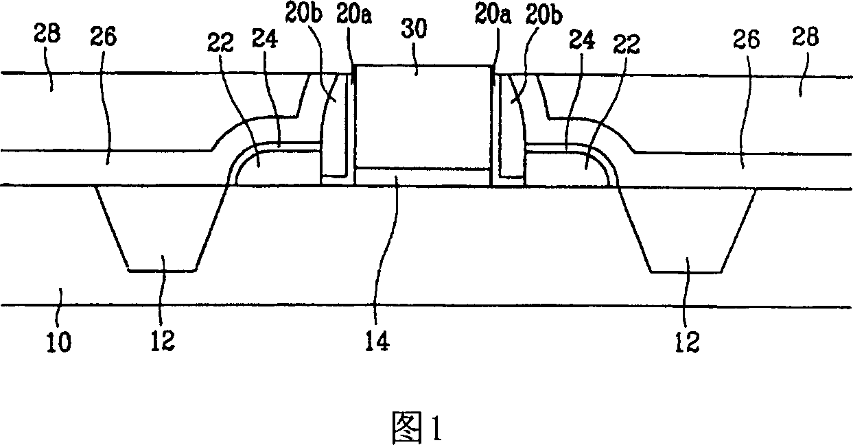
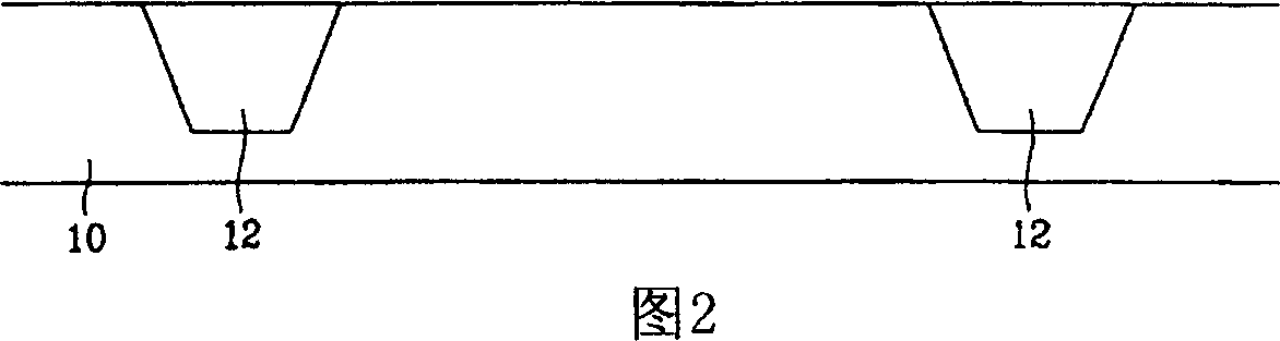
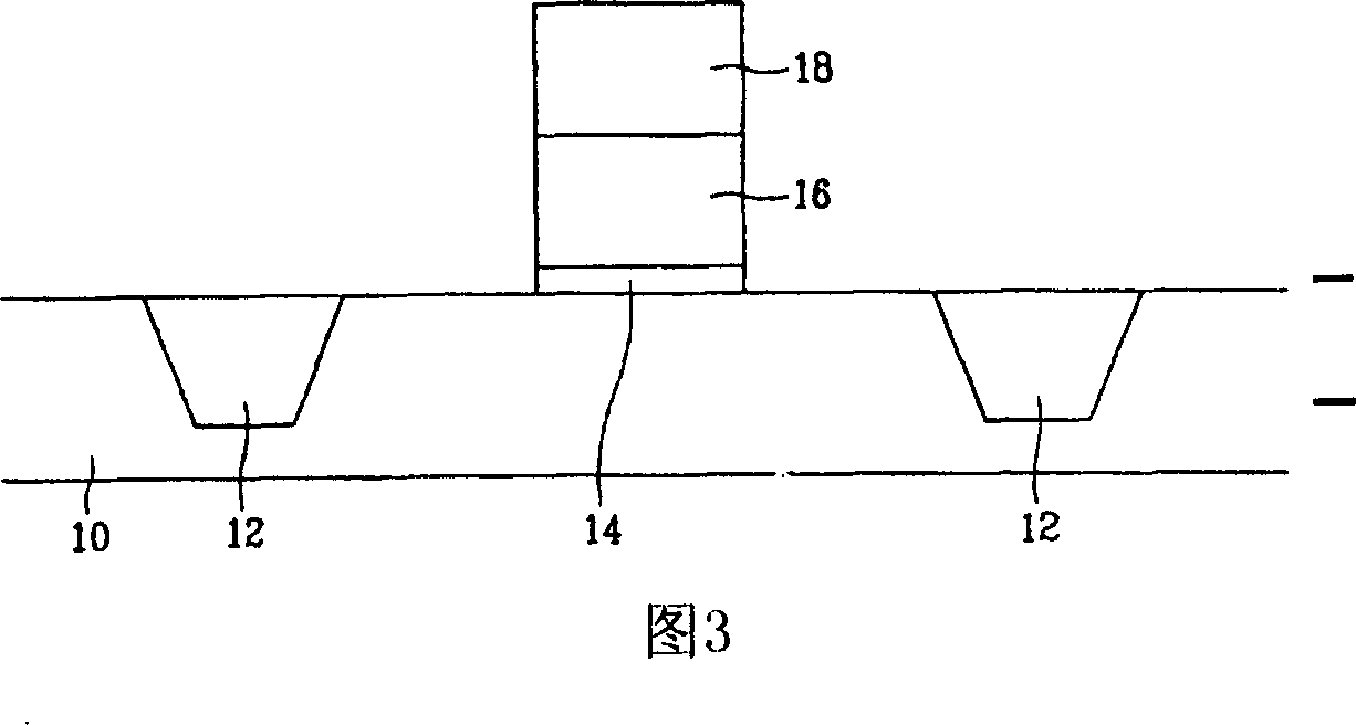
[0018] FIG. 1 is a cross-sectional ...
PUM
 Abstract
Description
Claims
Application Information
 - R&D Engineer
- R&D Manager
- IP Professional
- Industry Leading Data Capabilities
- Powerful AI technology
- Patent DNA Extraction
Browse by: Latest US Patents, China's latest patents, Technical Efficacy Thesaurus, Application Domain, Technology Topic, Popular Technical Reports.
© 2024 PatSnap. All rights reserved.Legal|Privacy policy|Modern Slavery Act Transparency Statement|Sitemap|About US| Contact US: help@patsnap.com